
A vertical mosfet transistor with a vertical capacitor region

a technology of capacitor region and mosfet, which is applied in the direction of basic electric elements, electrical equipment, and semiconductor devices, can solve the problems of limiting the efficiency of a voltage regulator by the time it takes for the drain current to be released, requiring a higher voltage (i.e. more expensive) power mosfet to be used, and reducing the risk of component failure. , the effect of compact pcb

Active Publication Date: 2014-08-07
NEXPERIA BV
View PDF6 Cites 26 Cited by
  • Summary
  • Abstract
  • Description
  • Claims
  • Application Information

AI Technical Summary

Benefits of technology

This solution effectively reduces total circuit inductance, improves switching speed, and enhances performance by integrating the bypass capacitor within the MOSFET dies, resulting in a more compact and cost-effective semiconductor package with reduced voltage spiking and EMI issues.

Problems solved by technology

A limiting factor in the efficiency of a voltage regulator is the time it takes for the drain current to rise and fall within the power MOSFETs used inside the regulator.
In addition to the need to reduce inductance to improve switching speed, the loop inductance is also responsible for generating voltage spikes that can cause problematical EMI, damage to driver and control ICs, and also require higher voltage (i.e. more expensive) power MOSFETs to be used (e.g. for 12V conversion, 30V MOSFETs are standard).
It is complex to manufacture, thus adding to the cost of the package.
In addition, the placement of the capacitor in between the MOSFET chips negatively impacts the current flow between these chips as it increases the metal resistance of the low side MOSFET, thus compromising the performance characteristics of the power converter.
Moreover, it is difficult to achieve such a capacitor with a sufficiently large capacitance in an economically feasible manner, as for such lateral capacitors the capacitance scales with A / d where A is the plate area and d is the distance between the plates, i.e. the thickness of the dielectric layer.

Method used


Image

  • A vertical mosfet transistor with a vertical capacitor region
  • A vertical mosfet transistor with a vertical capacitor region
  • A vertical mosfet transistor with a vertical capacitor region

Examples


Embodiment Construction

[0030]Embodiments of the invention are described in more detail and by way of non-limiting examples with reference to the accompanying drawings, wherein:

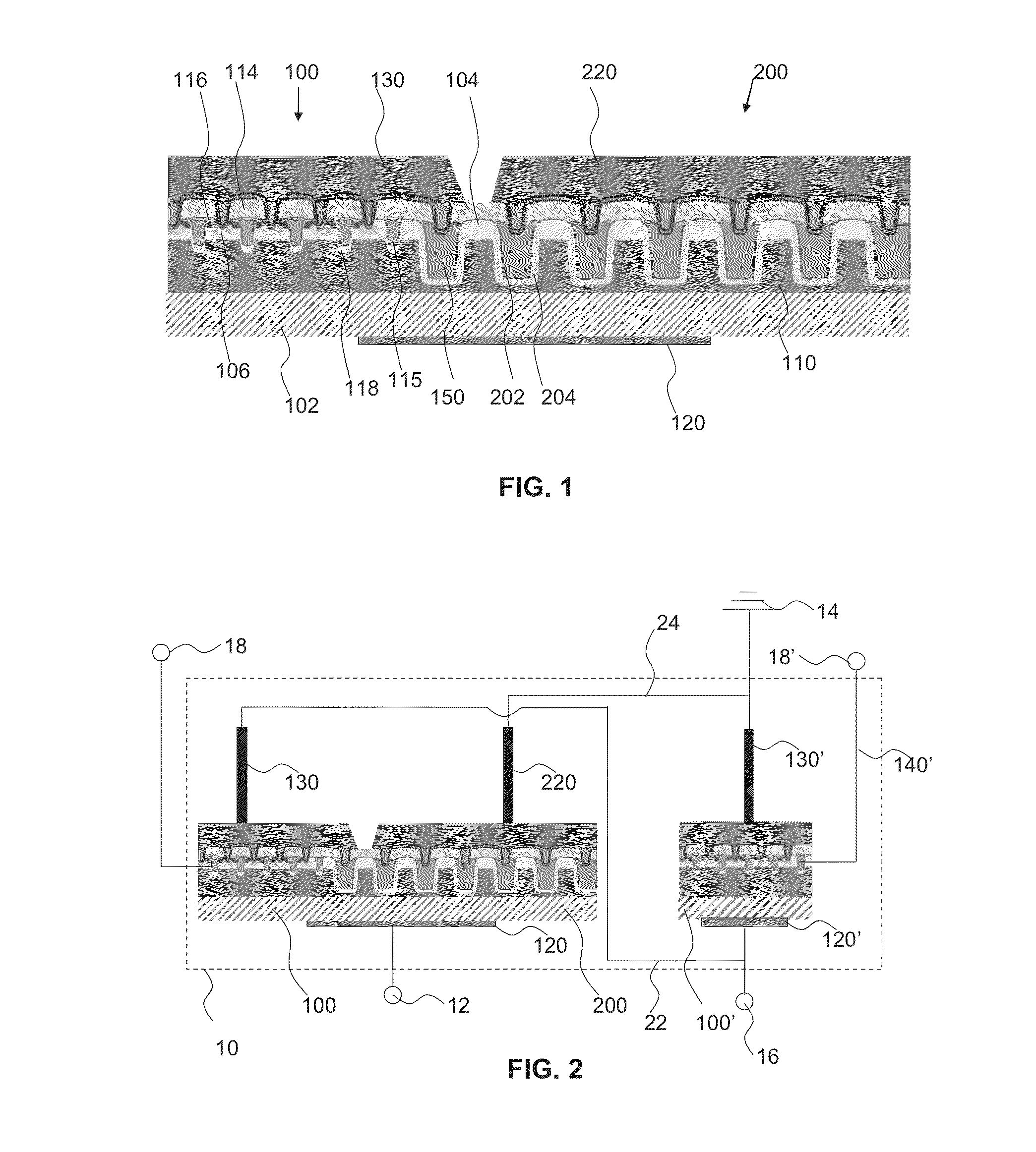
[0031]FIG. 1 schematically depicts a MOSFET die;

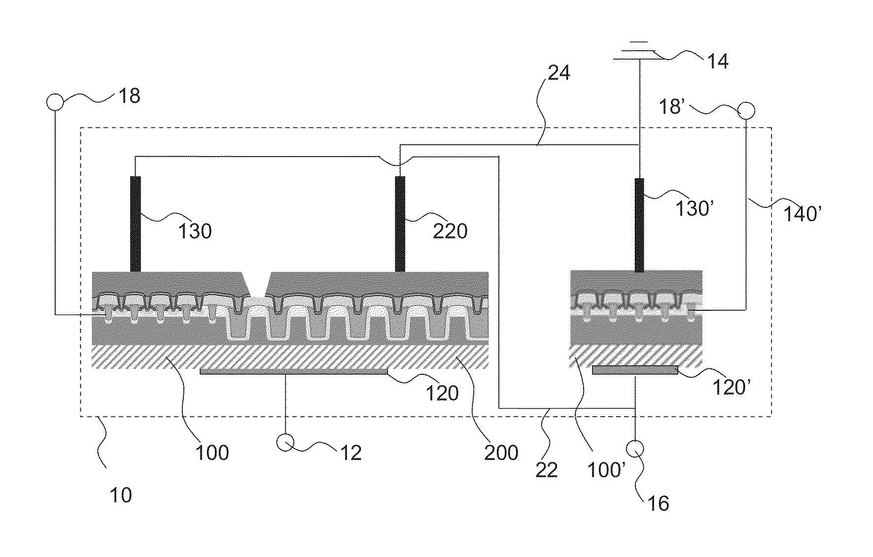
[0032]FIG. 2 schematically depicts a semiconductor package according to an embodiment of the present invention;

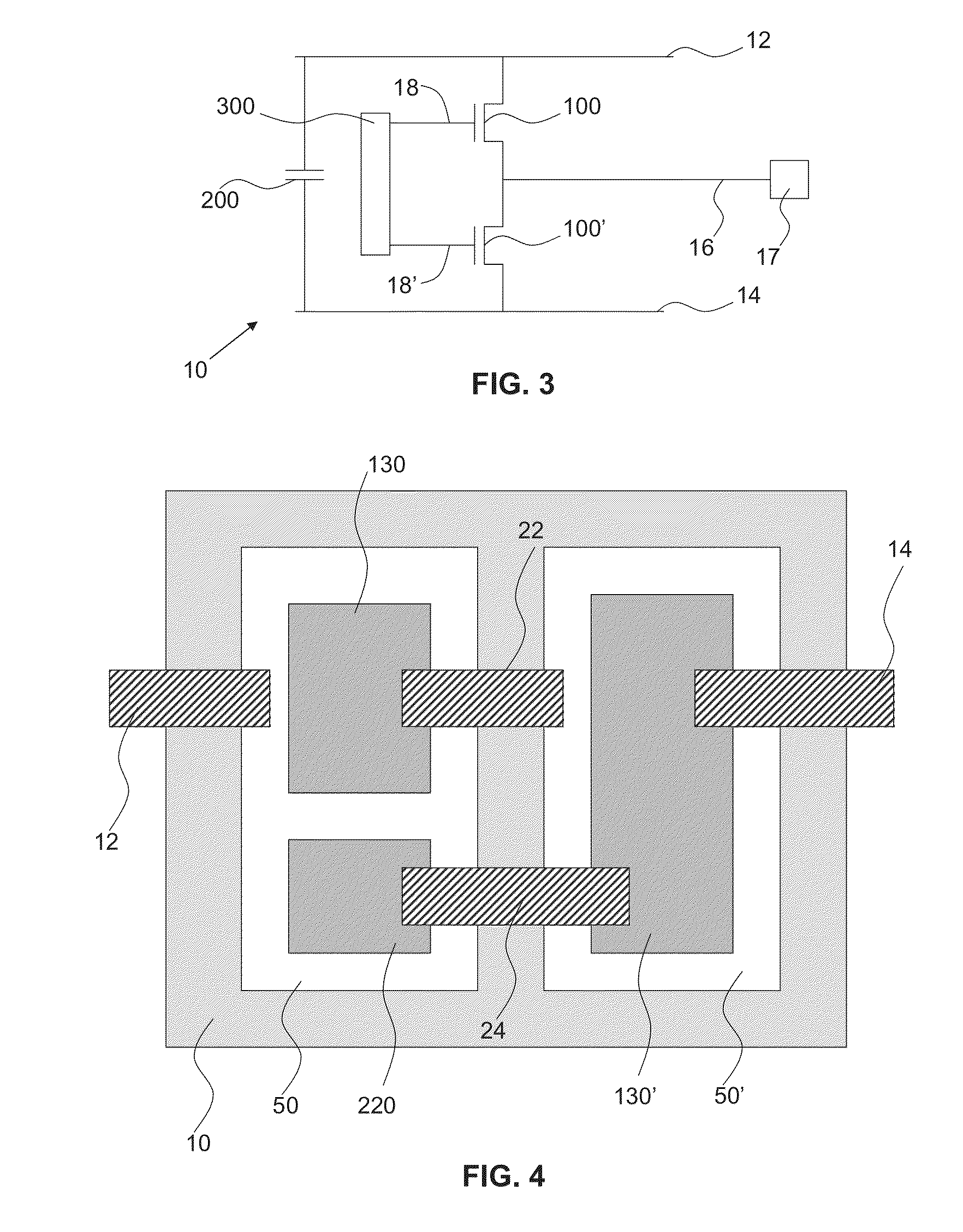
[0033]FIG. 3 schematically depicts a replacement schedule of the semiconductor package of FIG. 2; and

[0034]FIG. 4 schematically depicts an alternative view of the semiconductor package of FIG. 2.

DETAILED DESCRIPTION OF THE DRAWINGS

[0035]It should be understood that the Figures are merely schematic and are not drawn to scale. It should also be understood that the same reference numerals are used throughout the Figures to indicate the same or similar parts.

[0036]FIG. 1 shows a non-limiting example of a semiconductor die or chip in which a vertical MOSFET 100 and a vertical capacitor 200 are formed. The vertical MOSFET 100 comprises a drain region 102 and a source region 106 in b...


PUM


Abstract

Consistent with an example embodiment, a method of may be provided to manufacture a vertical capacitor region that comprises a plurality of said trenches, wherein the portions of the semiconductor region in between said trenches comprise an impurity. This allows for the trenches to be placed in closer vicinity to each other, thus improving the capacitance per unit area ratio. The total capacitance of the device is defined by two series components, that is, the capacitance across the dielectric liner, and the depletion capacitance of the silicon next to the trench. An increase of the voltage on the capacitor increases the depletion in the silicon and the depletion capacitance as a result, such that the overall capacitance is reduced. This effect may be countered by minimizing the depletion region which may be achieved by ensuring that the silicon adjacent to the capacitor is as highly doped as possible.

Description

FIELD OF THE INVENTION[0001]The present invention relates to a semiconductor package including a high side MOSFET (metal oxide semiconductor field effect transistor) coupled in series with a low side MOSFET between a first voltage terminal and a second voltage terminal.[0002]The present invention further relates to a PCB (printed circuit board) comprising such a semiconductor package.BACKGROUND OF THE INVENTION[0003]PCBs typically comprise discrete semiconductor components to achieve the desired functionality of the PCB. This typically includes a voltage regulator, which is used to provide the various components of the PCB with a constant voltage supply to ensure that these components do not display any undesirable behavior resulting from variations in their voltage supply. The voltage regulator may for instance be designed to convert an alternating current into a direct current.[0004]A popular embodiment of such a voltage regulator or power converter is a pair of serially connected...

Claims


Application Information

Patent Timeline
Patent Type & Authority Applications(United States)
IPC IPC(8): H01L29/66H10B12/00
CPCH01L29/66666H01L29/407H01L29/41766H01L29/42368H01L29/7803H01L29/7811H01L29/7813H01L27/0733H01L29/0661H01L25/072H01L2924/0002H01L2924/00H01L29/7827
Inventor RUTTER, PHILIP
Owner NEXPERIA BV
Learn More