
Method for manufacturing MEMS device

a manufacturing method and technology of mems, applied in the field of semiconductor manufacturing, can solve the problems of inability to react with polishing solutions, inability to use sacrificial materials in the sacrificial materials, and inability to use sacrificial materials, so as to avoid polishing amorphous carbon, reduce production cycle, and improve efficiency.

Active Publication Date: 2013-11-21
ZHEJIANG JUEXIN MICROELECTRONICS CO LTD
View PDF6 Cites 3 Cited by
  • Summary
  • Abstract
  • Description
  • Claims
  • Application Information

AI Technical Summary

Benefits of technology

The present patent provides methods for manufacturing MEMS devices that increase the speed of polishing sacrificial material and prevent over polishing. By forming and patterning the sacrificial layer before the dielectric layer, production cycle is reduced and efficiency is improved. This results in faster and more effective device manufacturing.

Problems solved by technology

However, these materials are unlikely to react with polishing solutions due to special chemical characteristics thereof.
As a result, the CMP process may have an unacceptable low polishing speed of the sacrificial material.
Besides, the polishing speed of the sacrificial material is much faster than that of the semiconductor dielectric layer, which may, on the one hand, prolong the polishing period, on the other hand, bring a difficulty for stopping the polishing precisely on the surface of the semiconductor dielectric layer.
A loss on the semiconductor dielectric layer's thickness is likely to occur.

Method used


Image

  • Method for manufacturing MEMS device
  • Method for manufacturing MEMS device
  • Method for manufacturing MEMS device

Examples


Embodiment Construction

[0041]In current MEMS manufacturing techniques, when forming a cavity for accommodating a suspended micro mechanical component, a groove is normally formed in advance, then a sacrificial material layer is filled into the groove to support upper structures. If inert substance like amorphous carbon is applied as the sacrificial material, it might be quite difficult to make the sacrificial material layer thinner using a conventional chemical mechanical polishing (CMP) process. In embodiments of the present disclosure, a sacrificial material layer with a desired thickness is directly formed and patterned, so that there is no need to perform a CMP on it.

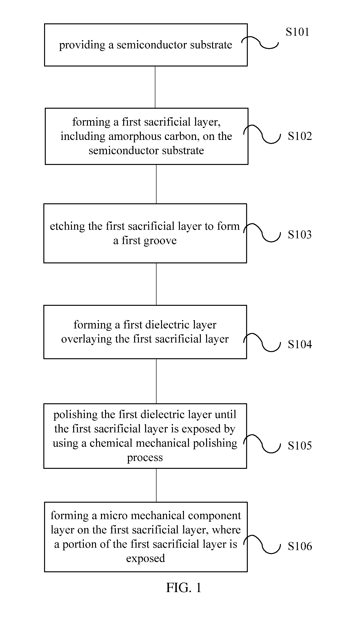
[0042]FIG. 1 schematically illustrates a flow chart of a method for forming a MEMS device according to one embodiment of the present disclosure, including steps of S101 to S106.

[0043]Step S101, providing a semiconductor substrate.

[0044]The semiconductor substrate constitutes a semiconductor substructure of the MEMS device, which may not b...


PUM

PropertyMeasurementUnit
Temperatureaaaaaaaaaa
Dielectric polarization enthalpyaaaaaaaaaa

Abstract

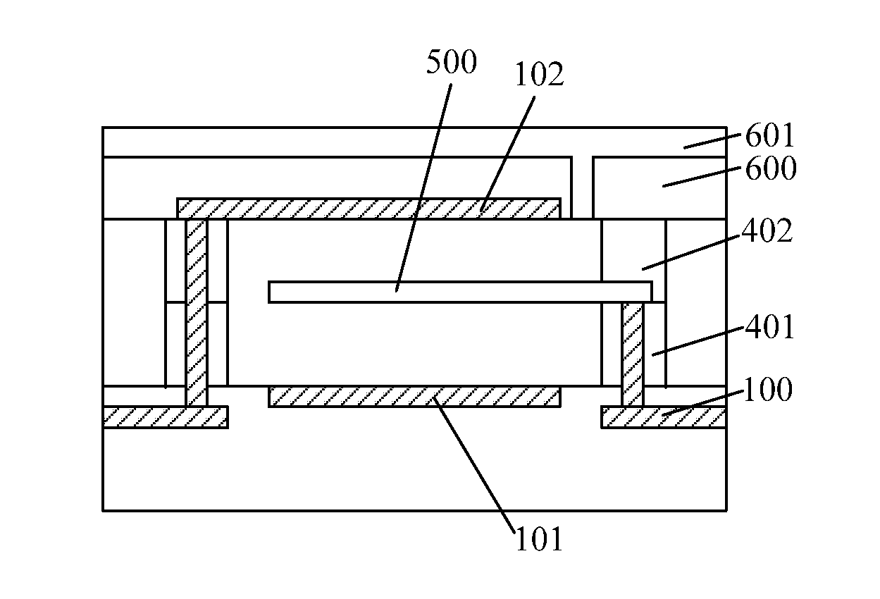
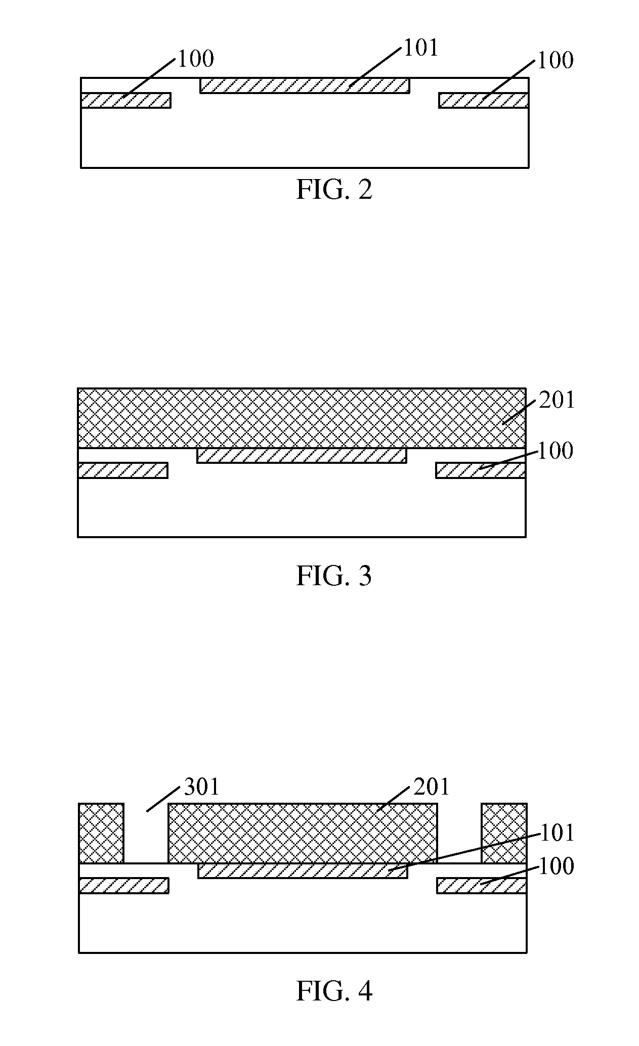
A method for manufacturing a micro-electro-mechanical system (MEMS) device is provided. The method comprises: providing a semiconductor substrate, the semiconductor substrate having a metal interconnection structure (100) formed therein; forming a first sacrificial layer (201) on the surface of the semiconductor substrate, the material of the first sacrificial layer is amorphous carbon; etching the first sacrificial layer to form a first recess (301); covering and forming a first dielectric layer (401) on the surface of the first sacrificial layer; thinning the first dielectric layer by a chemical mechanical polishing (CMP) process, until exposing the first sacrificial layer; forming a micromechanical structure layer (500) on the surface of the first sacrificial layer and exposing the first sacrificial layer, wherein a part of the micromechanical structure layer is connected to the first dielectric layer. The method avoids polishing the amorphous carbon, shortens the period of production, and improves the production efficiency

Description

CROSS REFERENCE TO RELATED APPLICATIONS [0001]The present application claims priority to Chinese patent application No. 201010607826.6, filed on Dec. 27, 2010, and entitled “Method for Manufacturing MEMS Device”, the entire disclosure of which is incorporated herein by reference.FIELD OF THE DISCLOSURE [0002]The present disclosure relates to semiconductor manufacturing, and more particularly, to a method for manufacturing a MEMS device.BACKGROUND OF THE DISCLOSURE [0003]Micro-Electro-Mechanical Systems (MEMS), which are suitable for integrated production, are micro devices or systems in which micro mechanisms, micro sensors, micro operators, and signal processing and control circuits are gathered as integral structures. MEMS are developed with the evolution of semiconductor integrated circuit precise manufacturing and super-precise mechanical manufacturing. Micro-electro devices applying MEMS technology are widely used in aviation, aerospace, environment supervision, biological medi...

Claims


Application Information

Patent Timeline
IPC IPC(8): B81C1/00
CPCB81C1/0015B81B2203/0118B81B2207/07B81C1/00293B81C2201/0109B81C2203/0145H03H3/0072B81C2201/0125G01P15/0802G01P2015/0828
Inventor MAO, JIANHONGTANG, DEMING
Owner ZHEJIANG JUEXIN MICROELECTRONICS CO LTD
Learn More