Eureka AIR delivers breakthrough ideas for toughest innovation challenges, trusted by R&D personnel around the world.

Monolithic parallel multijunction OLED with independent tunable color emission

a multijunction oled, independent technology, applied in the direction of organic semiconductor devices, solid-state devices, thermoelectric devices, etc., can solve the problems of increasing complexity of the fabrication process, requiring delicate vacuum handling and either evaporation or sputtering processes, and reducing the efficiency of charge injection

Inactive Publication Date: 2013-09-19
BOARD OF RGT THE UNIV OF TEXAS SYST +1
View PDF0 Cites 53 Cited by
  • Summary
  • Abstract
  • Description
  • Claims
  • Application Information

AI Technical Summary

Benefits of technology

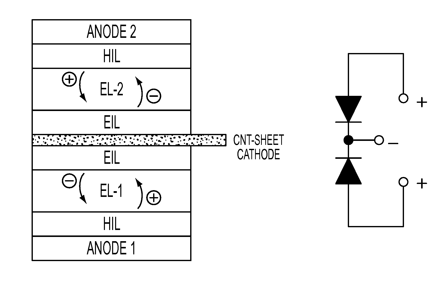
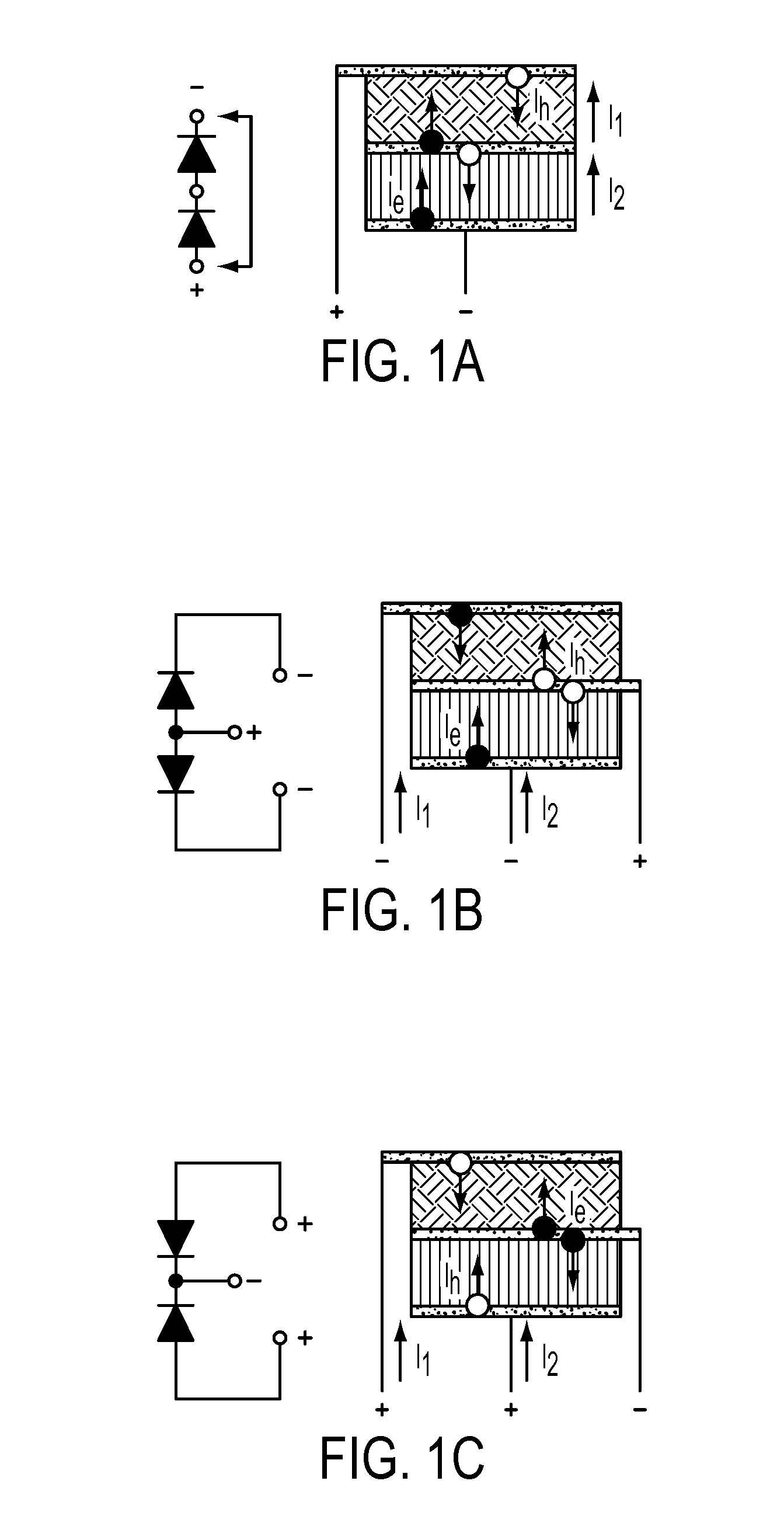
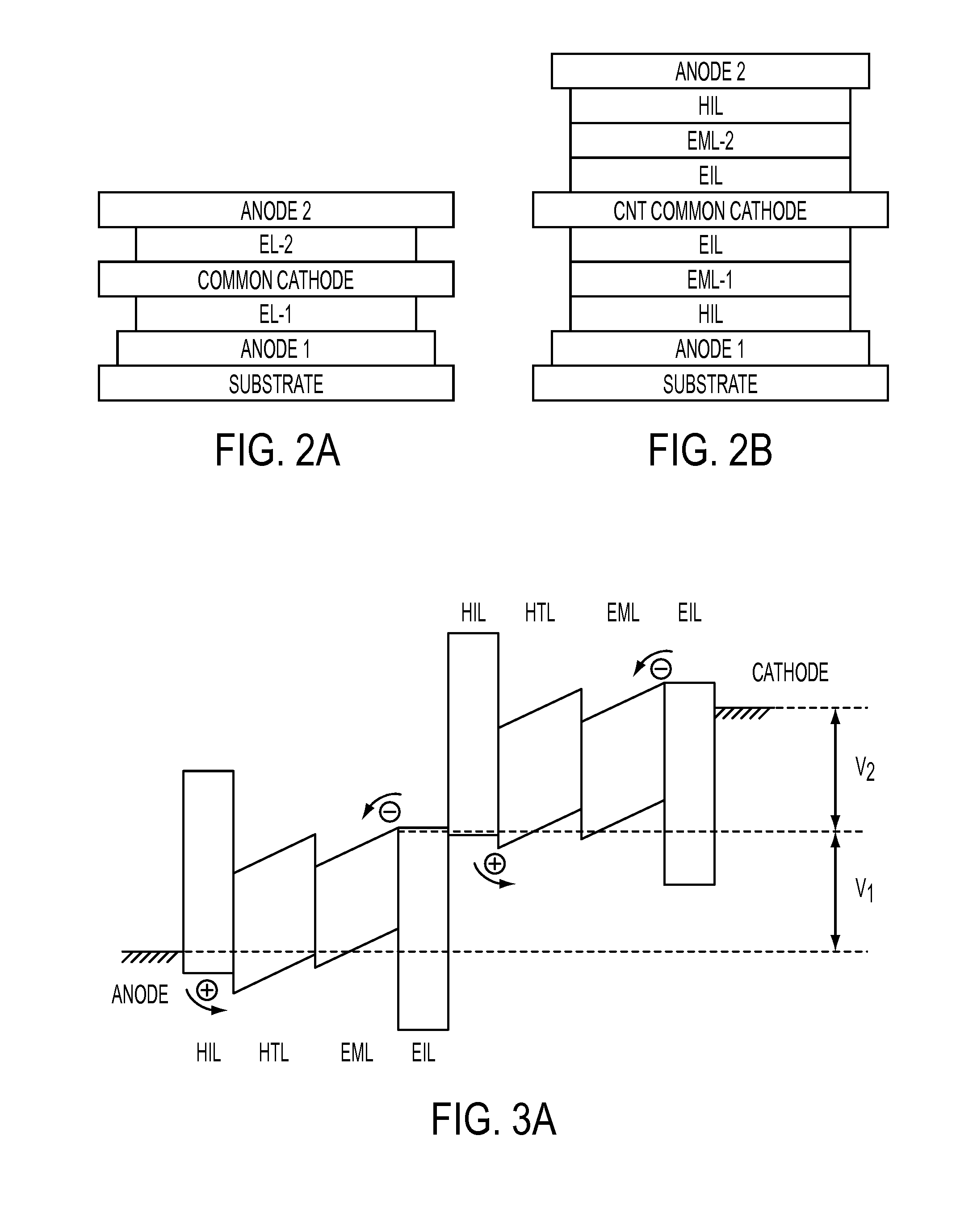
The invention is an OLED device that uses a transparent nanomaterial, such as carbon nanotubes or graphene sheets, as an interlayer between the electrodes. This interlayer acts as a conductor to improve the device performance. The device consists of several stacked electroluminescent units connected electrically in parallel, resulting in high intensity optical output with improved color quality. The device can be fabricated by combining complementary colors in a vertically stacked geometry. The invention introduces a new parallel configuration that combines the advantages of conventional in-series tandems with the benefits of a series connection. The design can be used to achieve tunable light emission of any color by separate voltage applied to each subunit. The functional character of the common electrode can be improved by doping the nanomaterial, adding inversion layers, or disposing injection layers adjacent to the interlayer. This allows for low operation voltage and high current injection.

Problems solved by technology

However, such structures require a complex interfacial layer between two emissive layers EML (1) and EML (2) which is critical for the device operation.
However, the fabrication of an interlayer between EML (1) and EML (2) requires delicate vacuum handling and either evaporation or sputtering processes.
Inevitably, the fabrication process becomes increasingly complicated.

Method used


Image

  • Monolithic parallel multijunction OLED with independent tunable color emission
  • Monolithic parallel multijunction OLED with independent tunable color emission
  • Monolithic parallel multijunction OLED with independent tunable color emission

Examples


working examples

Example 1

[0048]The process of dry-drawing of CNT sheets has been discovered by scientists at the Nanotech Institute of The University of Texas at Dallas and has been improved further by several groups, including those who emphasize the drawing of CNT yarns and fibers. Synthesis of CNT is done inside a three zone furnace with two inch diameter quartz tube will be utilized for Chemical Vapor Deposition (CVD) of CNT. Acetylene gas is inserted in a reactor at about 700° C. during the growth process. This CVD furnace will grow multi-walled carbon nanotubes (MWCNT) on the silicon wafer with iron catalyst deposited by e-beam deposition. After the CNT forest is grown on the silicon wafer, the forest can be pulled out and transferred as free standing CNT sheets. A CNT forest grown on the surface of a Si substrate is shown FIG. 11. A CNT sheet is then pulled off the forest and a continuous strand is formed. The CNT sheet it placed free standing on the CNT sheet holder as for storage and trans...

example 2

[0049]FIGS. 12 and 13 illustrate transparent OLEDs with CNT sheets. A transparent bottom cathode, similar to the ones described above, is fabricated on glass substrate. An emissive layer is deposited and then the CNT sheet is deposited to form the anode. In FIG. 12, the device structure is very similar to the bottom unit of tandem OLED, except that CNTs are not required to be placed between two hole injecting layers. FIG. 13 demonstrates another structure for transparent OLED devices. In this configuration, the CNT sheets are transferred on top of the transparent substrate. Next, a planarizing layer of PEDOT:PSS is spin casted before the active layer. The cathode is fabricated by deposition of transparent cathode on top that can be fabricated by bilayers of electron injecting materials (Ca, Mg, LiF, Cs, Bphen, Cs2CO3) and a metal (Ag,Al,Ni). A second layer of CNTs may be applied instead of the metal layer.

example 3

[0050]Flexible substrates are compatible with CNT sheets for flexible OLEDs. FIG. 14 illustrates a similar device to Example 2 (FIG. 13) but on a flexible substrate. Traditional transparent conductive oxides (such as ITO) are brittle and may crack under tension. CNT sheets have excellent mechanical and electrical properties and are excellent alternatives to ITO. CNT sheets are transferred on a polyethylene terephthalate (PET) substrate and the resulting surface is planarized prior the deposition of the emissive layer. An electron injection layer and the cathode are added to conclude the fabrication. The parallel tandem architecture of the claimed invention is compatible with flexible substrates and devices as shown in FIG. 10 can be fabricated in the same way.


PUM


Abstract

A tandem organic light emitting diode (OLED) device comprised of multiple stacked single OLEDs electrically connected in parallel via transparent interlayer is recited herein. Transparent interlayers are coated by charge injection layers in order to enhance the charge injection efficiency and decrease the operation voltage. Transparent nanomaterials, such as carbon nanotube sheets (or graphene, graphene ribbons and similar conductive transparent nano-carbon forms) are used as Interlayers or outer electrodes. Furthermore, functionalization of carbon nanotubes inter layers by n-doping (or p-doping) converts them into common cathode (or common anode), further decreasing operation voltage of tandem. The development of these alternative interconnecting layers comprised of nanomaterials simplifies the process and may be combined with traditional OLED devices. In addition, novel architectures are enabled that allow the parallel connection of the stacked OLEDs into monolithic multi-junction OLED tandems.

Description

CROSS-REFERENCES TO RELATED APPLICATIONS[0001]This application claims priority from U.S. Provisional Patent Application No. 61 / 347,272 filed May 21, 2010, which is hereby incorporated by reference as if fully set forth herein.STATEMENT REGARDING FEDERALLY-SPONSORED RESEARCH OR DEVELOPMENT[0002]This invention was made with government support under Grant No. DE-SC0001145 and Grant No. DE-SC0003664 awarded by the Department of Energy. The government has certain rights in the invention.BACKGROUND OF INVENTION[0003]An organic light-emitting diode device, also called an OLED, commonly includes an anode, a cathode, and an organic electroluminescent (EL) unit sandwiched between the anode and the cathode. Generally, at least one of the electrodes is transparent. The organic EL unit may be comprised of a single electroluminescent material in the case of polymer based OLEDs. Also, in the case of small molecule OLEDs it may include a hole-transporting layer (HTL), a light-emitting layer (EML), ...

Claims


Application Information

Patent Timeline
IPC IPC(8): H01L51/52H01L51/56
CPCH01L27/3202H01L27/3209H01L51/5206H01L51/5234H01L51/56H01L2251/5338H01L2251/564B82Y40/00H01L51/5203H01L51/5296H10K59/84H10K59/32H10K50/81H10K50/828H10K50/19H10K50/30H10K71/841H10K2102/311H10K50/805H10K71/00
Inventor ZAKHIDOV, ANVAR A.PAPADIMITRATOS, ALEXIOS
Owner BOARD OF RGT THE UNIV OF TEXAS SYST
Why Eureka
Eureka Blog
Learn More