Method to Shorten Crystal Oscillator's Startup Time
a crystal oscillator and startup time technology, applied in the field of crystal oscillators, can solve the problems of low startup time, control loop, high phase noise performance, etc., and achieve the effect of shortening the startup time of the oscillator, automatic amplitude control, and open loop gain of aa
- Summary
- Abstract
- Description
- Claims
- Application Information
AI Technical Summary
Benefits of technology
Problems solved by technology
Method used
Image
Examples
first embodiment
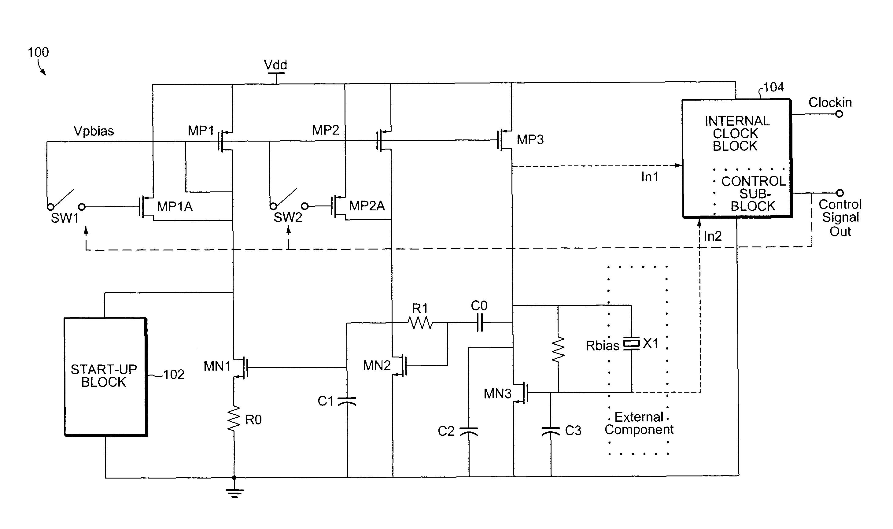
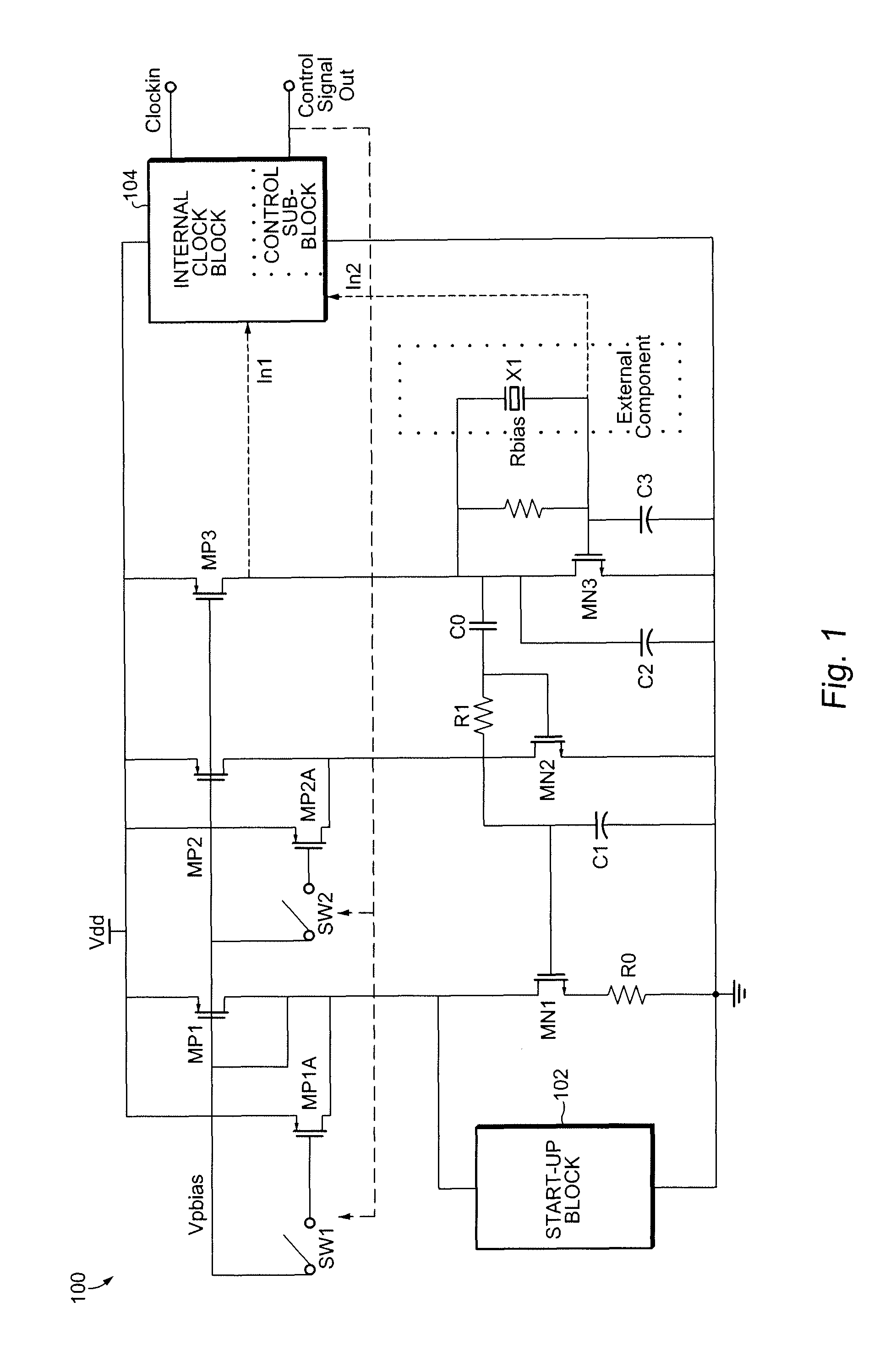
[0013]Referring now to FIG. 1 an oscillator circuit 100 according to the present invention comprises an amplifier, an AAC loop, a startup circuit 102, an internal clock block 104 including a control signal block, as well as controlled switches and transistors. The Pierce crystal oscillator circuit 100 further comprises a crystal (X1, which is generally an external component), load capacitors (C2 coupled to the drain of transistor MN3 and C3 coupled to the gate of transistor MN3), and a bias resistor (Rbias) across the crystal.
[0014]The amplifier includes transistors MN3 and MP3. The AAC loop includes transistors MN1, MN2, MP1 (and MP1A), MP2 (and MP2A), R0, Co, R1 and C1. Capacitor C0 is a DC-blocking capacitor, which couples the oscillating signal from the drain of transistor MN3. The combination of resistor R1 and capacitor C1 is a low-pass filter. A self bias circuit is formed by transistors MN1, MN2, MP1, MP2 and resistor R0. The bias transistor is split up into two parts by a s...
second embodiment
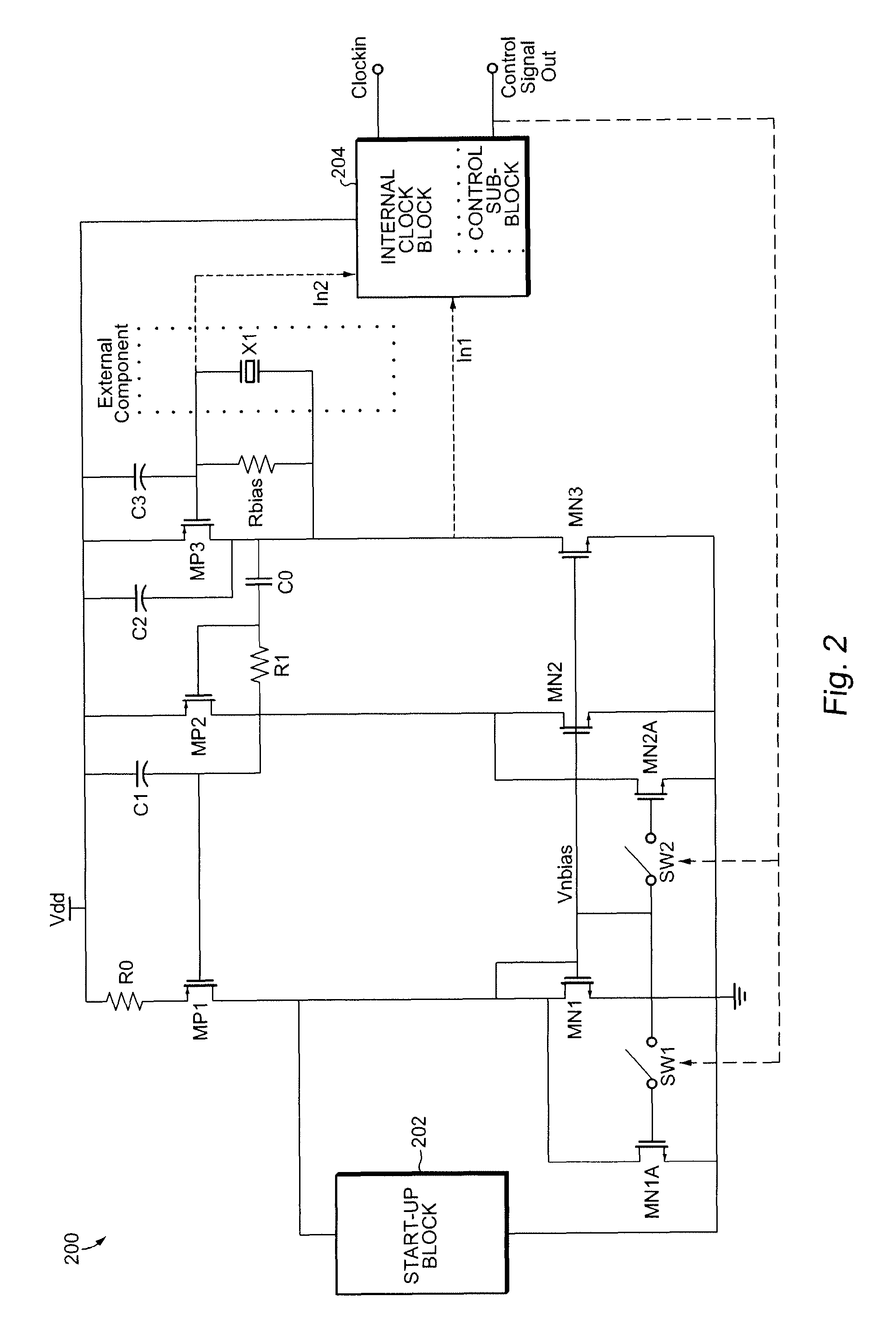
[0022]Referring now to FIG. 2 an oscillator circuit 200 according to the present invention comprises an amplifier, an AAC loop, a startup circuit 202, an internal clock block 204 including a control signal block, as well as controlled switches and transistors. The Pierce crystal oscillator circuit 200 further comprises a crystal (X1, which is generally an external component), load capacitors (C2 coupled to the drain of transistor MP3 and C3 coupled to the gate of transistor MP3), and a bias resistor (Rbias) across the crystal.
[0023]The amplifier includes transistors MN3 and MP3. The AAC loop includes transistors MN1 (and MN1A), MN2 (and MN2A), MP1, MP2, R0, Co, R1 and C1. Capacitor C0 is a DC-blocking capacitor, which couples the oscillating signal from the drain of transistor MN3. The combination of resistor R1 and capacitor C1 is a low-pass filter. A self bias circuit is formed by transistors MN1, MN2, MP1, MP2 and resistor R0. The bias transistor is split up into two parts by a s...
third embodiment
[0028]In the invention, the circuit shown in FIG. 1 can be “flipped” as is known in the art, wherein the PMOS and NMOS transistors are swapped, the polarities of the signals changed, and the power and ground rails are switched.
PUM
 Abstract
Description
Claims
Application Information
 - R&D
- Intellectual Property
- Life Sciences
- Materials
- Tech Scout
- Unparalleled Data Quality
- Higher Quality Content
- 60% Fewer Hallucinations
Browse by: Latest US Patents, China's latest patents, Technical Efficacy Thesaurus, Application Domain, Technology Topic, Popular Technical Reports.
© 2025 PatSnap. All rights reserved.Legal|Privacy policy|Modern Slavery Act Transparency Statement|Sitemap|About US| Contact US: help@patsnap.com


