Buffer Layer for GaN-on-Si LED

a buffer layer and led technology, applied in the field of gan-on-si led buffer layers, can solve the problems of gallium-nitride substrate wafers, non-monochromatic and non-coherent light, and other substrates, which are still undetectable, and achieve the effects of reducing the cost of manufacturing blue leds, reducing lattice defect density, and easy preparation

Inactive Publication Date: 2013-03-07
KK TOSHIBA
View PDF5 Cites 14 Cited by
  • Summary
  • Abstract
  • Description
  • Claims
  • Application Information

AI Technical Summary

Benefits of technology

[0015]Platinum is a quite expensive metal, whereas titanium is substantially less expensive. The prior art wafer bonding process described above in the background section involves five or more platinum layers, each of which may be 100 nm or more in thickness. The prior art process uses 500 nm or more of platinum. By reducing the amount of platinum used to a single layer that is thinner than 200 nm, the novel non-reactive metal bonding process disclosed here can reduce the cost of manufacturing blue LEDs on silicon substrates.
[0016]In a third novel aspect, a blue LED device is manufactured by epitaxially growing an n-type Gallium-Nitride (GaN) layer over a silicon substrate using Zinc-Sulfide (ZnS) as a transitional buffer layer. In one example, the ZnS buffer layer is 50 nm thick, and the n-type GaN layer is at least 2000 nm thick. Growing the n-type GaN layer on the ZnS buffer layer reduces lattice defect density in the n-type GaN layer. First, the ZnS buffer layer provides a good lattice constant match with the silicon substrate and a compound polar template for subsequent GaN growth. Second, ZnS can be easily prepared by metal-organic chemical vapor deposition (MOCVD) such that all the epilayers are grown in one growth chamber. Third, the melting point of ZnS is 1850° C., which is high enough to keep it from becoming unstable during GaN deposition. Finally, if an aluminum-nitride (AlN) layer is also used as part of the buffer layer, then the ZnS layer is used as a diffusion barrier between the AlN layer and the silicon substrate. After the epitaxial layers of the epitaxial LED structure are formed, a carrier wafer structure is wafer bonded to the structure where the carrier wafer structure includes a conductive carrier. The original silicon substrate and the ZnS buffer layer are then removed from the wafer bonded structure. Electrodes are added and the wafer bonded structure is singulated to form finished LED devices.

Problems solved by technology

Some emit laser light, and others generate non-monochromatic and non-coherent light.
Although gallium-nitride substrate wafers are available, they are very expensive.
These other substrates are, however, still undesirably expensive.
It therefore would be desirable from a cost point of view to be able to fabricate GaN-based LEDs on relatively inexpensive silicon substrate wafers and to use the available second-hand semiconductor processing equipment for processing such silicon wafers, but there are many problems with growing high quality GaN epitaxial layers on silicon substrates.
Many of the problems associated with growing high quality GaN epitaxial layers on silicon substrates derive from the fact that the lattice constant of silicon is substantially different from the lattice constant of GaN.
When GaN is grown epitaxially on a silicon substrate, the epitaxial material being grown may exhibit an undesirably high density of lattice defects.
If the GaN layer is grown to be thick enough, then stress within the GaN layer may result in a type of cracking in the latter-grown portions of the GaN material.
These different rates of thermal expansive give rise to stress between the various layers of the LED device.
This stress may cause cracking and other problems.
Furthermore, it is difficult to grow GaN on a silicon substrate because GaN is a compound material and Si is an elemental material.
The transition from nonpolar to polar structure, combined with the substantial lattice mismatch, generates defects.

Method used


Image

  • Buffer Layer for GaN-on-Si LED
  • Buffer Layer for GaN-on-Si LED
  • Buffer Layer for GaN-on-Si LED

Examples


Embodiment Construction

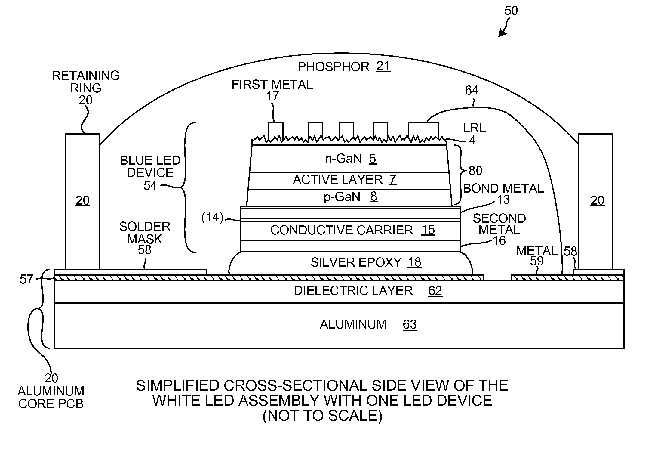
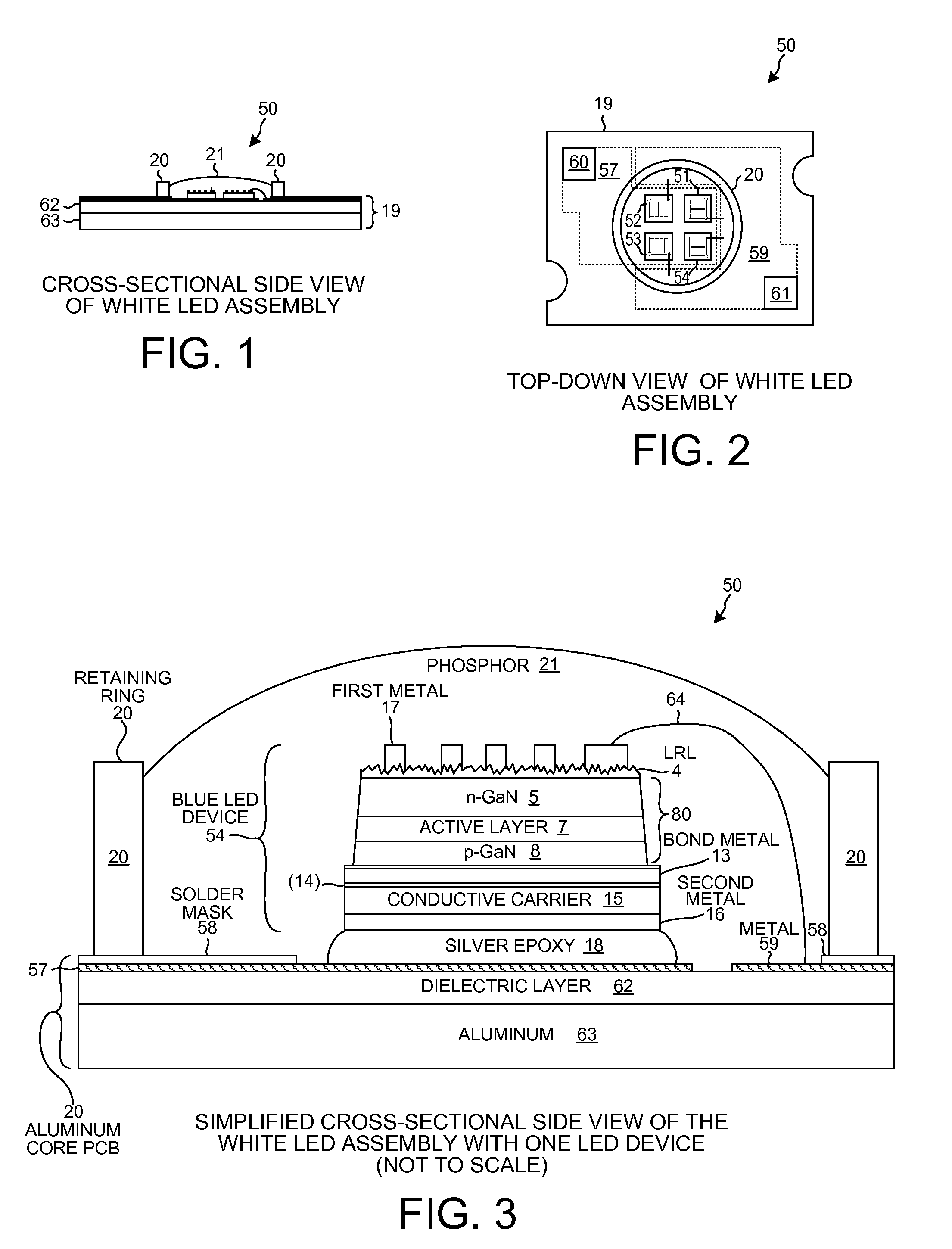
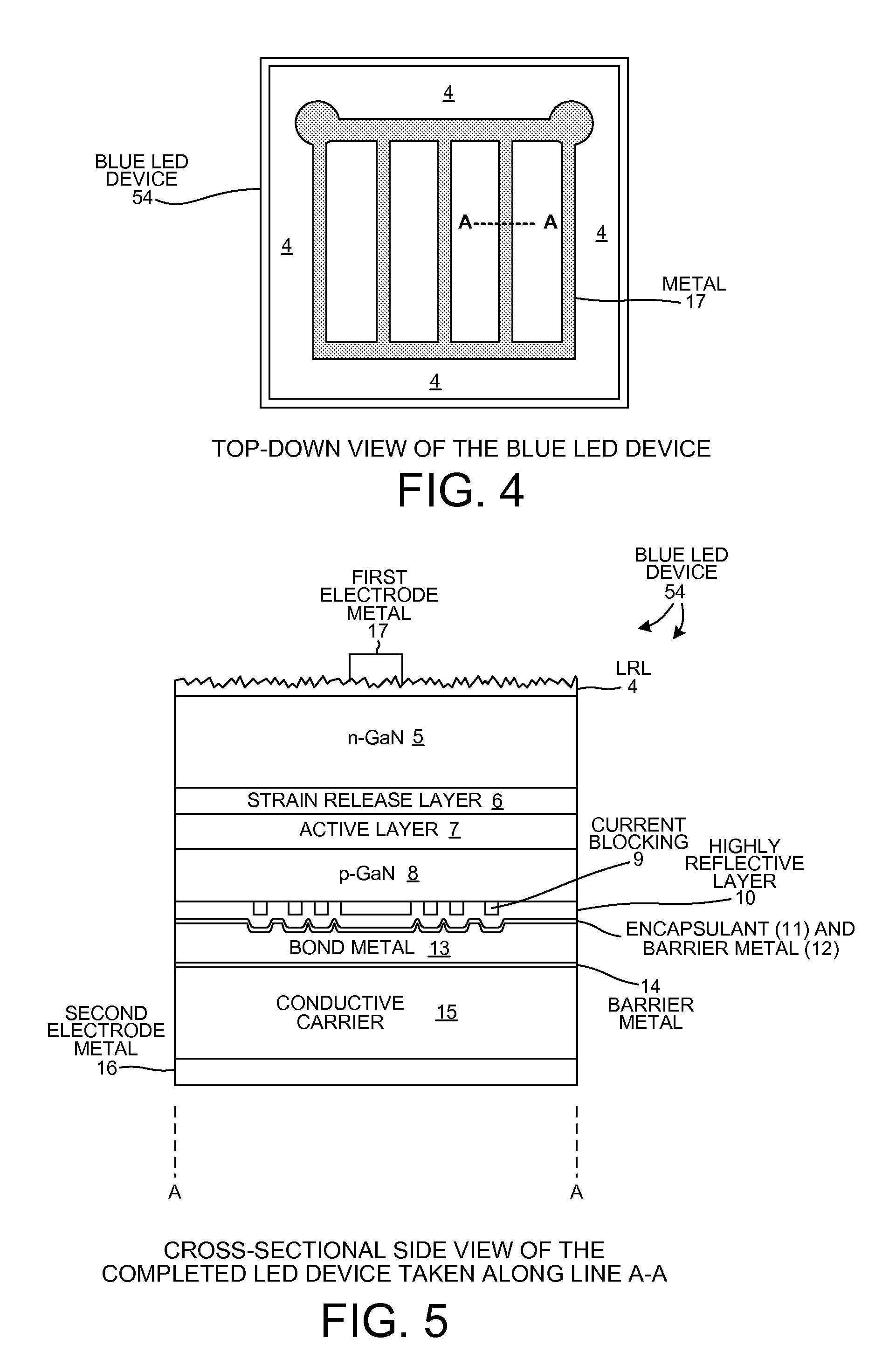
[0048]Reference will now be made in detail to some embodiments of the invention, examples of which are illustrated in the accompanying drawings. In the description and claims below, when a first layer is referred to as being disposed “over” a second layer, it is to be understood that the first layer can be directly on the second layer, or an intervening layer or layers may be present between the first and second layers. The terms such as “over”, “under”, “upper”, “lower”, “top”, “bottom”, “upward”, “downward”, “vertically”, and “laterally” are used herein to describe relative orientations between different parts of the blue LED device being described, and it is to be understood that the overall blue LED device being described can actually be oriented in any way in three-dimensional space.

[0049]FIG. 1 is a cross-sectional side view of a white light emitting diode (LED) assembly 50. FIG. 2 is a top-down diagram of the white LED assembly 50. The white LED assembly 50 includes four vert...


PUM

PropertyMeasurementUnit
thickaaaaaaaaaa
thicknessaaaaaaaaaa
wavelengthaaaaaaaaaa

Abstract

A buffer layer of zinc telluride (ZnTe) or titanium dioxide (TiO2) is formed directly on a silicon substrate. Optionally, a layer of AlN is then formed as a second layer of the buffer layer. A template layer of GaN is then formed over the buffer layer. An epitaxial LED structure for a GaN-based blue LED is formed over the template layer, thereby forming a first multilayer structure. A conductive carrier is then bonded to the first multilayer structure. The silicon substrate and the buffer layer are then removed, thereby forming a second multilayer structure. Electrodes are formed on the second multilayer structure, and the structure is singulated to form blue LED devices.

Description

TECHNICAL FIELD[0001]The present disclosure relates generally to GaN-based blue LEDs manufactured on silicon substrates and related methods and structures.BACKGROUND INFORMATION[0002]A Light Emitting Diode (LED) is a solid state device that converts electrical energy to light. Light is emitted from an active layer of semiconductor materials sandwiched between oppositely doped layers when a voltage is applied across the doped layers. There are many different LED device structures that are made of different materials and have different structures and that perform in different ways. Some emit laser light, and others generate non-monochromatic and non-coherent light. Some are optimized for performance in particular applications. Some are high power devices and others are not. Some emit light as infrared radiation, whereas others emit visible light of various colors, and still others emit ultraviolet light. Some are expensive to manufacture, whereas others are less expensive. For commerc...

Claims


Application Information

Patent Timeline
Patent Type & Authority Applications(United States)
IPC IPC(8): H01L33/32H01L33/48
CPCH01L21/02381H01L21/0248H01L21/02488H01L33/12H01L33/007H01L33/0079H01L21/0254H01L2224/2929H01L2224/29339H01L2224/48091H01L2224/73265H01L33/0093H01L2924/00014
Inventor CHEN, ZHEN
Owner KK TOSHIBA
Why Eureka
Try Eureka