Dislocation and stress management by mask-less processes using substrate patterning and methods for device fabrication

a substrate patterning and stress management technology, applied in the direction of semiconductor devices, basic electric elements, electrical equipment, etc., can solve the problems of reducing the performance of the device, so as to reduce minimize the density of the threading. , the effect of reducing the density of the threading

Active Publication Date: 2013-02-14
PILEGROWTH TECH
View PDF13 Cites 51 Cited by
  • Summary
  • Abstract
  • Description
  • Claims
  • Application Information

AI Technical Summary

Benefits of technology

[0049]The present invention provides means for fabricating active layer stacks of lattice matched, lattice mismatched and thermally mismatched materials on patterned substrates in mask-less processes. Substrates are patterned in the form of elevated regions, separated by narrow channels, the depths of which may exceed the smallest dimensions of elevated regions. A combination of elastic stress relaxation, and elimination of threading dislocations by annihilation, glide toward...

Problems solved by technology

Elastic relaxation cannot, however, proceed on a flat film.
Whenever an interface with a significant density of misfit dislocations is incorporated in the active region of a device, e.g., a transistor, its performance may be degraded to a large extent.
Unfortunately, however, keeping interfaces with misfit dislocations at a distance from the active region of a device often does not guarantee its proper performance.
Also these threading dislocations can be very detrimental to the functioning of a device if they traverse the active region of a heteroepitaxially grown layer stack.
Problems Related to Thermal Expansion Mismatch
In many instances the mismatch of the thermal expansion coefficients is equally serious, especially when layers with relatively large thicknesses are needed, for example in devices like high-brightness light emitting diodes for general lighting purposes, multiple junction solar cells, radiation detectors, thermoelectric generators, and many more.
The mismatch of thermal expansion coefficients may lead to wafer bowing upon cooling to room temperature after the epitaxial growth, seriously hampering subsequent processing steps, such as photolithography and patterning, or also further epitaxial growth.
Unfortunately, however, reducing wafer bowing may even increase the tendency of the overlayer to crack, because wafer bowing is associated with partial elastic stress relief.
While wafer bowing and layer cracking are severe practical problems arising typically at layer thicknesses beyond 1 μm, threading dislocations, intimately related to plastic strain relaxation, are normally present already at smaller layer thickness for significant lattice misfits of the order of a fraction of a percent or more.
The method does not, however, solve the problem of wafer bowing and crack formation, when Ge in the form of blanket films is grown to substantial thicknesses of several micrometers, and the TDD still remains very high, of the order of typically 2-107 cm−2 for 1 μm thick films.
Whenever epitaxial layers are grown in the form of continuous films onto a substrate characterized by a significant lattice and thermal expansion mismatch, one is faced with the problems of excessive TDD as soon as the misfit strain starts relaxing plastically, as well as wafer bowing and crack formation at larger thicknesses.
Limited area epitaxy, even when combined with thermal annealing, is not, however, sufficient by itself for complete removal of threading dislocations, even when feature sizes are kept very small.
Obviously, however, the problems of wafer bowing and layer cracking would come into play upon increasin...

Method used


Image

  • Dislocation and stress management by mask-less processes using substrate patterning and methods for device fabrication
  • Dislocation and stress management by mask-less processes using substrate patterning and methods for device fabrication
  • Dislocation and stress management by mask-less processes using substrate patterning and methods for device fabrication

Examples


examples

Substrate Patterning

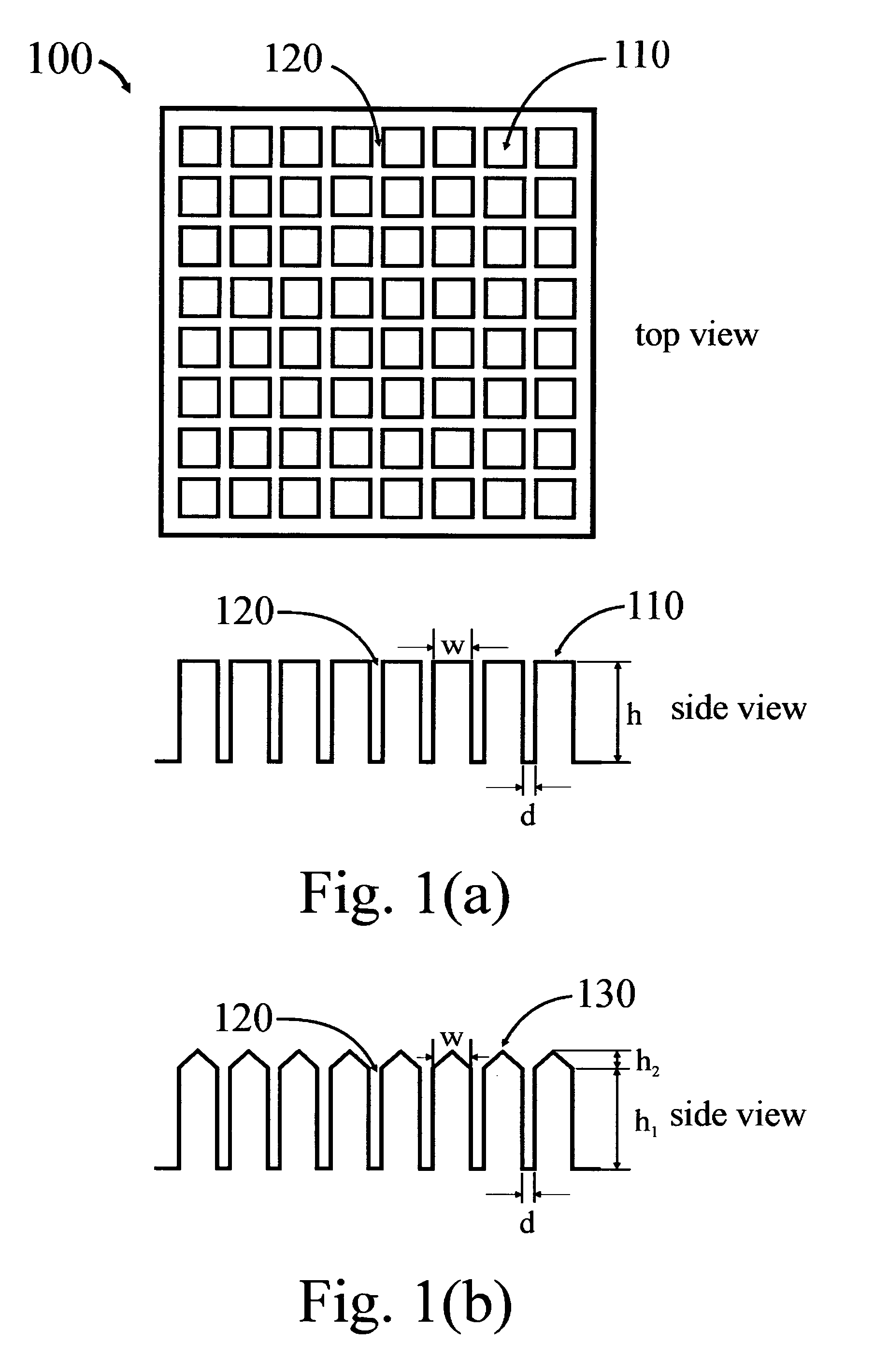
[0105]Referring now to FIGS. 8(a)-8(c), scanning electron microscopy (SEM) images 800 of patterned substrates may be seen in perspective (a) and plan (b)-(c) view. Here, the substrate is a Si(001) wafer which was patterned by standard photolithography and the Bosch process, leading to the ripples on the side walls of Si pillars 810. In FIG. 8(a) pillars 810 are about 1.8 μm wide, while the width of trenches 812 is about 2.2 μm. The plan view SEM image of FIG. 8(b) shows two different kinds of trenches with widths of about 1.7 μm for narrow trenches 830 and 2.9 μm for wider trenches 840, while pillars 820 are about 1.3 μm wide. Wider trenches 840 are about 8 μm deep, and narrow trenches 830 slightly less.

[0106]FIG. 8(c) shows other examples of patterns, A1, B1, C1 and D2, composed of elevated substrate regions 850, 860, 870 and 880 of different size and distance. Many more substrate patterns have been examined with elevated features ranging from submicron to tens ...


PUM


Abstract

Structures and methods for producing active layer stacks of lattice matched, lattice mismatched and thermally mismatched semiconductor materials, with low threading dislocation densities, no layer cracking and minimized wafer bowing, by using epitaxial growth onto elevated substrate regions in a mask-less process.

Description

CROSS REFERENCE TO RELATED APPLICATIONS[0001]This application claims the benefit of U.S. Provisional Application No. 61 / 328,203, filed 27 Apr. 2010, the content of which is incorporated herein by reference and relied upon.FIELD OF THE INVENTION[0002]The invention relates to structures and methods for eliminating threading dislocations, layer cracking and wafer bowing in the epitaxial growth of lattice mismatched and thermally mismatched layers by using patterned substrates. Since materials choice and layer thicknesses are virtually unlimited, the invention can be applied also to the fabrication of devices requiring thick epilayers for their proper functioning, such as multiple junction solar cells, light emitting diodes, semiconductor lasers, radiation imaging detectors and thermo-electric devices. The invention is viable also for the fabrication of microelectronic, opto-electronic and photonic circuits requiring smaller thicknesses of mismatched epilayers.BACKGROUND OF THE INVENTIO...

Claims


Application Information

Patent Timeline
IPC IPC(8): H01L29/12H01L21/20
CPCH01L21/0237H01L21/02381H01L21/0243H01L21/0265H01L21/02532H01L21/02546H01L21/02639H01L21/02521H01L21/20H01L21/02
Inventor VON KANEL, HANSMIGLIO, LEONIDA
Owner PILEGROWTH TECH
Why Eureka
Try Eureka