
Process for producing multilayer chip zinc oxide varistor containing pure silver internal electrodes and firing at ultralow temperature

a technology of pure silver internal electrodes and multi-layer chips, applied in the direction of varistors, resistors, varistors, etc., can solve the problems of less adjustable properties of the resultant zno varistor, c value, surge-absorbing ability, esd-absorbing ability, etc., and achieve cost saving

Inactive Publication Date: 2012-05-31
SFI ELECTRONICS TECH
View PDF25 Cites 14 Cited by
  • Summary
  • Abstract
  • Description
  • Claims
  • Application Information

AI Technical Summary

Benefits of technology

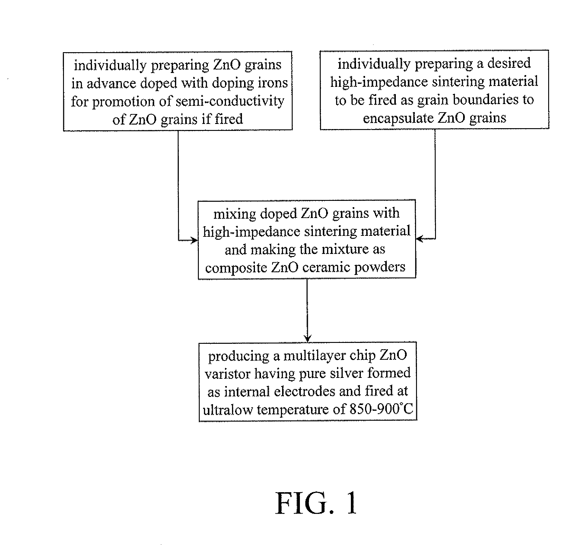
[0009]An object of the present invention is to provide a low-temperature firing process for producing multilayer chip ZnO varistor, and particularly, through the process of the present invention pure silver (Ag) can be formed as internal electrodes of the multilayer chip ZnO varistor, and more particularly the process for producing multilayer chip ZnO is capably fired at ultralow firing temperature of 850-900° C. for cost saving.
[0011]According to the present invention disclosed, the multilayer chip ZnO varistor may contain pure silver (Ag) formed as internal electrodes and the pure silver (Ag) internal electrodes can still provide excellent chemical stability during sintering at firing temperature of 850-900° C. below the Melting point of silver, so that the process for producing multilayer chip ZnO varistor of the present invention has completely improved the known conventional process for producing multilayer chip ZnO varistor commonly disclosed to exploit a silver / palladium alloy formed as an internal electrode.
[0019]2. according to the same reason mentioned above, an effective reduction of manufacture cost for producing multilayer chip ZnO varistor is also realized.

Problems solved by technology

Nevertheless, since formation of the high-impedance grain boundaries processed in the above-mentioned conventional process requires a relatively higher firing temperature than 1000° C. or more, the shortcoming of conventional process for producing ZnO varistors is that properties of the resultant ZnO varistor are less adjustable.
Consequently, properties of the resultant ZnO varistor, including breakdown voltage, nonlinear coefficient, C value, leakage current, surge-absorbing ability, and ESD-absorbing ability, are restricted.
Hence, because selectiveness of composition and quantity of the high-impedance grain boundaries is limited, improvement in technical conditions of the resultant ZnO varistors is unachievable and properties of the resultant ZnO varistors are rather inflexible.
In particular, the current multilayer chip ZnO varistor in market is commonly used a silver / palladium alloy (containing 70 wt % silver and 30 wt % palladium) formed as an internal electrode, resulted in that the firing temperature is reached to a comparatively high temperature of 1000° C.-1300° C. Since the multilayer chip ZnO varistor must use 20-30 wt % palladium (Pd) and be fired at relatively high temperature, the manufacturing cost is rather high.

Method used


Image

  • Process for producing multilayer chip zinc oxide varistor containing pure silver internal electrodes and firing at ultralow temperature
  • Process for producing multilayer chip zinc oxide varistor containing pure silver internal electrodes and firing at ultralow temperature
  • Process for producing multilayer chip zinc oxide varistor containing pure silver internal electrodes and firing at ultralow temperature

Examples


example 1

[0053]A mixture is prepared by taking 97.5% of ZnO doped with doping irons (which is stamped as sample O2 and hereinafter referred to as ZnO*) well to mix with 0.5% of Bi2O3, 1.0% of Sb2O3, 0.5% of CO2O3 and 0.5% of MnO2, all based on the mixture by weight.

[0054]The ZnO* grains of sample O2 is prepared by immersing fine ZnO powders into a solution containing doping ions of Sn, Al and Si and encompasses 1 mol % of ZnO, 0.006 mol % of SnO2, 0.00015 mol % of Al2O3 and 0.002 mol % SiO2 after sintered at 900° C. for two hours.

[0055]The mixture after further ground into fine powders was used to make a disc-shaped ZnO varistor with diameter of 8 mm under pressure of 1000 kg / cm2. And then, the produced disc-shaped varistor was sintered at 850° C. for five hours to obtain the final product. At last, the varistor properties of the disc-shaped varistor, including breakdown voltage (abbreviated as “BDV”), nonlinear exponent (α) and leakage current (iL), are measured, and the measured results ar...

example 2

[0059]The chemical coprecipitation method was used to prepare a sintering material numbered G-100, which has the composition as provided in Table 2 below.

[0060]Taking ZnO* grains of example 1 well to mix with the sintering material of 0-100 to form a mixture after in advance sintered at 750° C. for five hours.

[0061]And, the mixture was used to make disc-shaped ZnO varistors under the same conditions as provided in Example 1, The varistors were tested on their varistor properties and the results are listed in Table 3.

TABLE 2Composition of Sintering Material G-100SinteringComposition (mol %)MaterialBi2O3Sb2O3MnOCo2O3Cr2O3SiO2B2O3TiO2Y2O3G-1003.52.52.52.82.51.01.01.50.1

TABLE 3Properties of ZnO Varistors Made of grains boundaries preparedby chemical coprecipitationBDV(V / mm)αiL (μA)Before ESD Test113943.0111.0After ESD test by116622.0736.930 KV strike 200 times

[0062]From Table 3, it is learned that the varistor properties, particular in respects of BDV, of disc-shaped ZnO varistors is ob...

example 3

[0063]Taking ZnO* grains of Example 1 but sintered at 1,200° C. for six hours instead. Further mixing the ZnO* grains of this example with the sintering material of G-100 of Example 2 in a weight ratio of 90:10, 80:20 or 70:30 respectively to form three kinds of mixture after in advance sintered at 800° C. for five hours.

[0064]And, each mixture was used to make disc-shaped ZnO varistors under the same conditions as provided in Example 1. Each varistor was respectively tested on their varistor properties and the results are listed in Table 4.

TABLE 4Properties of ZnO varistors varied with the quantity of grain boundariesWeight ratio of ZnO* / BDViLSurgesintering material(V / mm)α(μA)(A)90:1042115.5031.450080:2033720.3212.480070:3033924.156.50900

[0065]From Table 4, it is learned that the BDV value of disc-shaped ZnO varistors is obviously reduced by increase of sintering temperature of ZnO* grains doped with doping irons. In addition, the ZnO varistors have their varistor properties varyin...


PUM

PropertyMeasurementUnit
temperatureaaaaaaaaaa
melting pointaaaaaaaaaa

Abstract

A low-temperature firing process is available for cost saving to produce a multilayer chip ZnO varistor containing pure silver (Ag) formed as internal electrodes and calcined at ultralow firing temperature of 850-900° C., which process comprises:a) individually preparing ZnO grains in advance doped with doping ions for promotion of semi-conductivity of ZnO grains if calcined;b) individually preparing a desired high-impedance sintering material to be fired as grain boundaries to encapsulate ZnO grains;c) mixing the doped ZnO grains of Step a) with the high-impedance sintering material of Step b) in a predetermined ratio to form a mixture and proceeding with an initial sintering to have the mixture sintered and ground as composite ZnO ceramic powders, andd) processing the sintered mixture of Step c) to make multilayer chip ZnO varistors containing pure silver (Ag) internal electrodes but sintered at ultralow firing temperature of 850-900° C.

Description

BACKGROUND OF THE INVENTION[0001]1. Field of the Invention[0002]The present invention relates to a process for producing multilayer chip zinc oxide (ZnO) varistor containing pure silver (Ag) formed as internal electrodes, more particularly to a process for producing the multilayer chip zinc oxide (ZnO) varistor at ultralow firing temperature of 850-900° C.[0003]2. Description of Prior Art[0004]Traditionally, a zinc oxide (ZnO) varistor is made by sintering zinc oxide, together with other oxides, such as antimony oxide, silicon oxide, cobalt oxide, manganese oxide and chrome oxide, at a firing temperature higher than 1000° C. During sintering, semi-conductivity of the ZnO grains increases due to the doping of Sb, Si, Co, Mn and Cr while a crystalline phase of high-impedance grain boundaries is deposited among the ZnO grains.[0005]Therefore, a conventional process for producing ZnO varistors is only disclosed a single sintering procedure to accomplish the following two purposes for a ...

Claims


Application Information

Patent Timeline
Patent Type & Authority Applications(United States)
IPC IPC(8): H01L21/02
CPCH01C7/18H01C7/112C04B35/453C04B2235/3267B32B18/00C04B2235/3217C04B2235/3241C04B2235/3275C04B2235/3279C04B2235/3284C04B2235/3294C04B2235/3298C04B2235/3418C04B2237/34C04B2237/68H01C7/1006H01C1/142
Inventor LIEN, CHING-HOHNZHU, JIE-AN
Owner SFI ELECTRONICS TECH
Learn More