
Ultra-thin interposer assemblies with through vias

a technology of interposer assemblies and vias, which is applied in the direction of electrical apparatus contruction details, printed circuit non-printed electric components association, and semiconductor/solid-state device details, etc. it can solve the problems of increasing the number of chip-to-chip interconnections, preventing these structures from providing high bandwidths without significant increase in power consumption, and cannot scale to multiple chips or sub-systems

Active Publication Date: 2012-05-03
GEORGIA TECH RES CORP
View PDF15 Cites 166 Cited by
  • Summary
  • Abstract
  • Description
  • Claims
  • Application Information

AI Technical Summary

Benefits of technology

[0012]Further exemplary embodiments of the present invention provide ease of thermal management interposer interconnect structure, comprising: an interposer having a first side and a second side; and a plurality of through-vias defined within the interposer extending at least from the first side to the second side of the interposer; and wherein the interposer electrically connects first and second electronic devices on either side of the through-via and has the same or substantially the same through-via interconnect density as the first and second electronic devices it connects; and further wherein the first and second electronic devices are connected by a plurality of electrically and thermally conducting through-vias, wherein the plurality of through-vias are distributed within the interposer and provide localized thermal isolation or thermal conduction between the first and second electronic devices.

Problems solved by technology

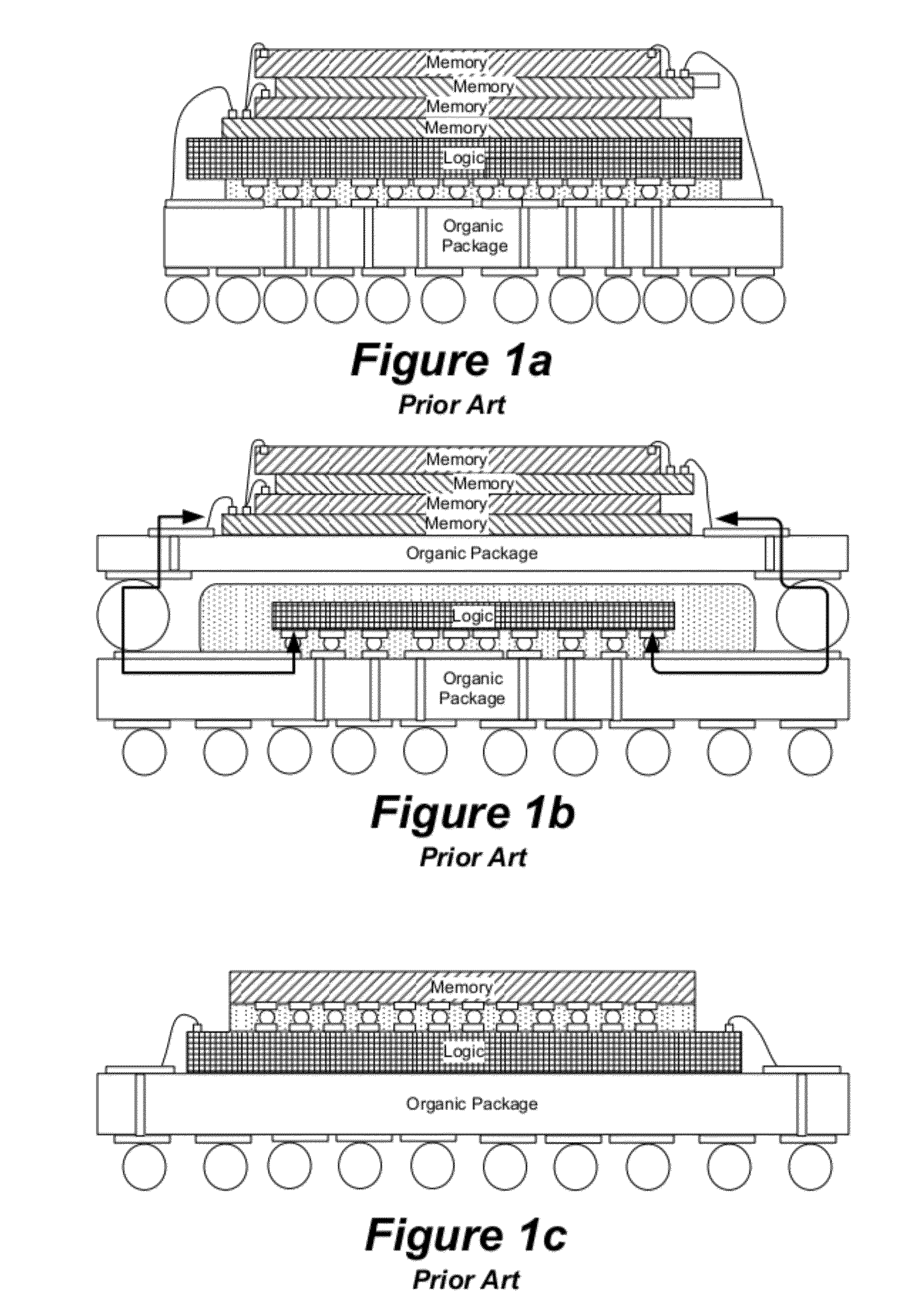
The wire-bonded SIP and POP structures are limited in the number of chip-to-chip interconnections and the interconnection length, preventing these structures from providing high bandwidths without a significant increase in power consumption.
The F2F structure achieves finer-pitch I / Os and thus increases the number of chip-to-chip interconnections, however, the design is limited to two chips and therefore cannot be scaled to multiple chips or sub-systems.
Such a structure has two limitations, however.
First, this structure is very expensive to manufacture, attributed to the small number of interposers produced from 200-300 mm wafers as well as the expensive back-end-of-line (BEOL) processes.
The second limitation is related to the electrical signal delay, due to both electrical lossiness of silicon as well the long wire lengths with high resistance.
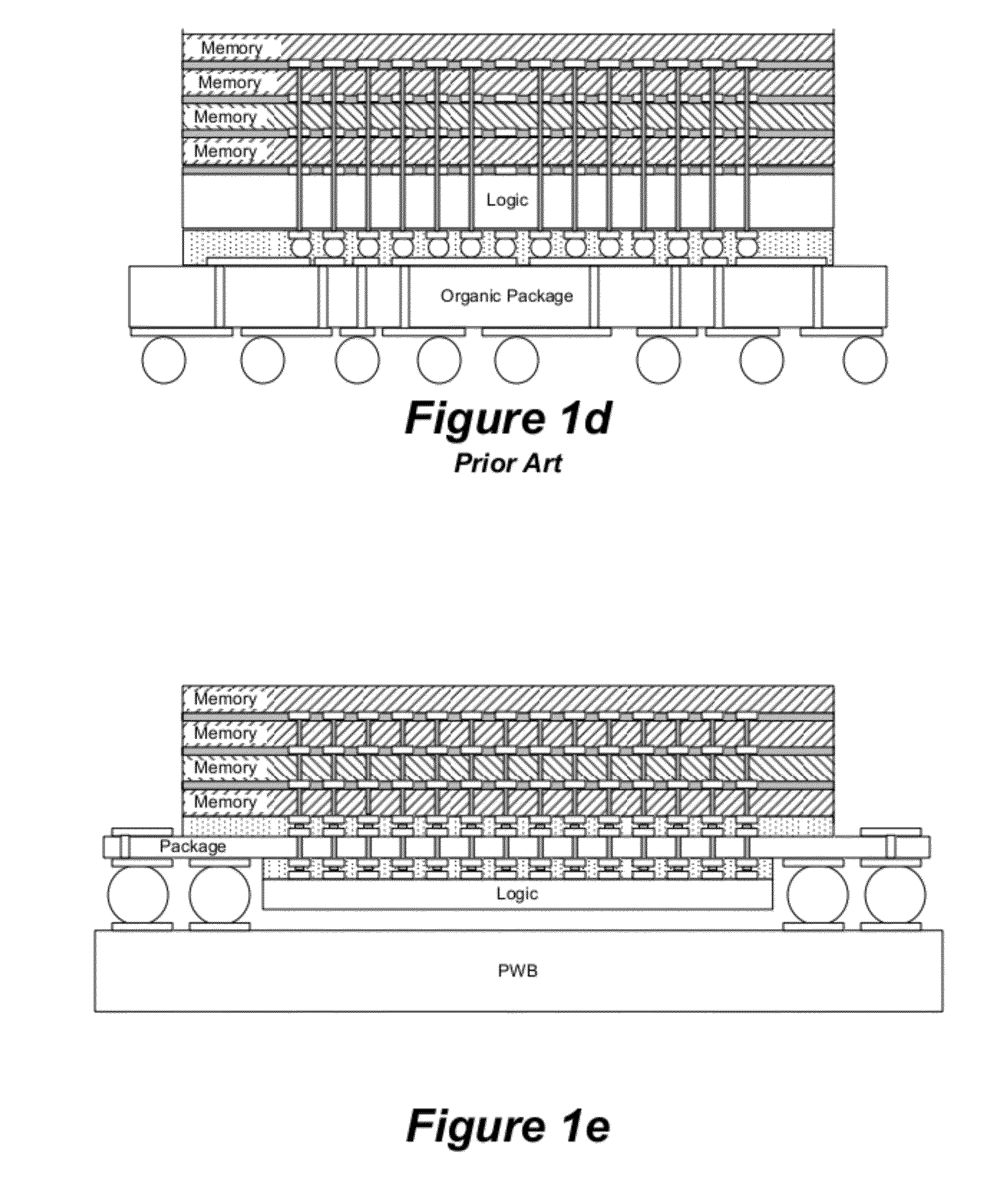
However, this form of multi-die stacking with TSVs imposes great challenges in forming TSVs within complementary metal oxide semiconductor (CMOS) chips, power delivery, testability, reliability, and thermal management of logic chip, all of which remain major barriers in achieving high bandwidth for 3D ICs.
Additionally, organic, ceramic, and glass carriers having conductive through vias have been described in prior art, however, they do not operate at high bandwidths because of coarse pitch and long interconnections.

Method used


Image

  • Ultra-thin interposer assemblies with through vias
  • Ultra-thin interposer assemblies with through vias
  • Ultra-thin interposer assemblies with through vias

Examples


example # 3

Example #3

TPV Fabrication Process

[0087]FIG. 23 illustrates the process flow used to fabricate the TPV in a polycrystalline silicon panel.

example # 4

Example #4

TPV Formation

[0088]Several methods for TPV formation in polycrystalline silicon were explored as the traditional DRIE processes are too slow to drill TPVs in silicon interposers of about 220 μm thick polycrystalline silicon. To solve this problem, TPV formation by laser ablation (UV, excimer and pico-second lasers) was studied. Top and bottom views of the vias fabricated by three types of lasers are compared in FIG. 24.

[0089]The UV laser with a wavelength of about 266 nm was faster but resulted in large via entrance diameters ranging from about 75-125 μm. The via exit diameter (ranging from about 50-100 μm) was smaller than the entrance diameter, indicating significant via taper. The excimer laser was able to drill smaller vias (about 10-20 μm diameter) than the UV laser. The excimer laser was able to form nearly vertical TPV sidewall without micro-cracking due to minimal thermal damage to the silicon material. Excimer laser processing can be scaled to higher throughput by...

example # 5

Example #5

Polymer filling and Liner Formation

[0091]A novel polymer liner approach is presented to replace the current combination of SiO2 and diffusion barriers used in the processing of CMOS-based silicon interposers. The technical approach involves polymer filling of TPV, followed by laser ablation to form an “inner” via resulting in a via side wall liner of controlled thickness.

[0092]The laser drilled silicon samples were first cleaned using a plasma treatment. About 30 μm thick polymer film was laminated to cover the surface and fill the TPVs. This was done by an optimized double-side lamination process with hot press, resulting in void-free filling without cracking the silicon. FIG. 26 shows the optical cross-sectional image of polymer laminated silicon substrate with polymer-filled TPV (about 125 μm and about 100 μm via entrance and exit diameter respectively). Adhesion between polymer and silicon was checked by initial tape test for peel strength and the samples showed good a...


PUM


Abstract

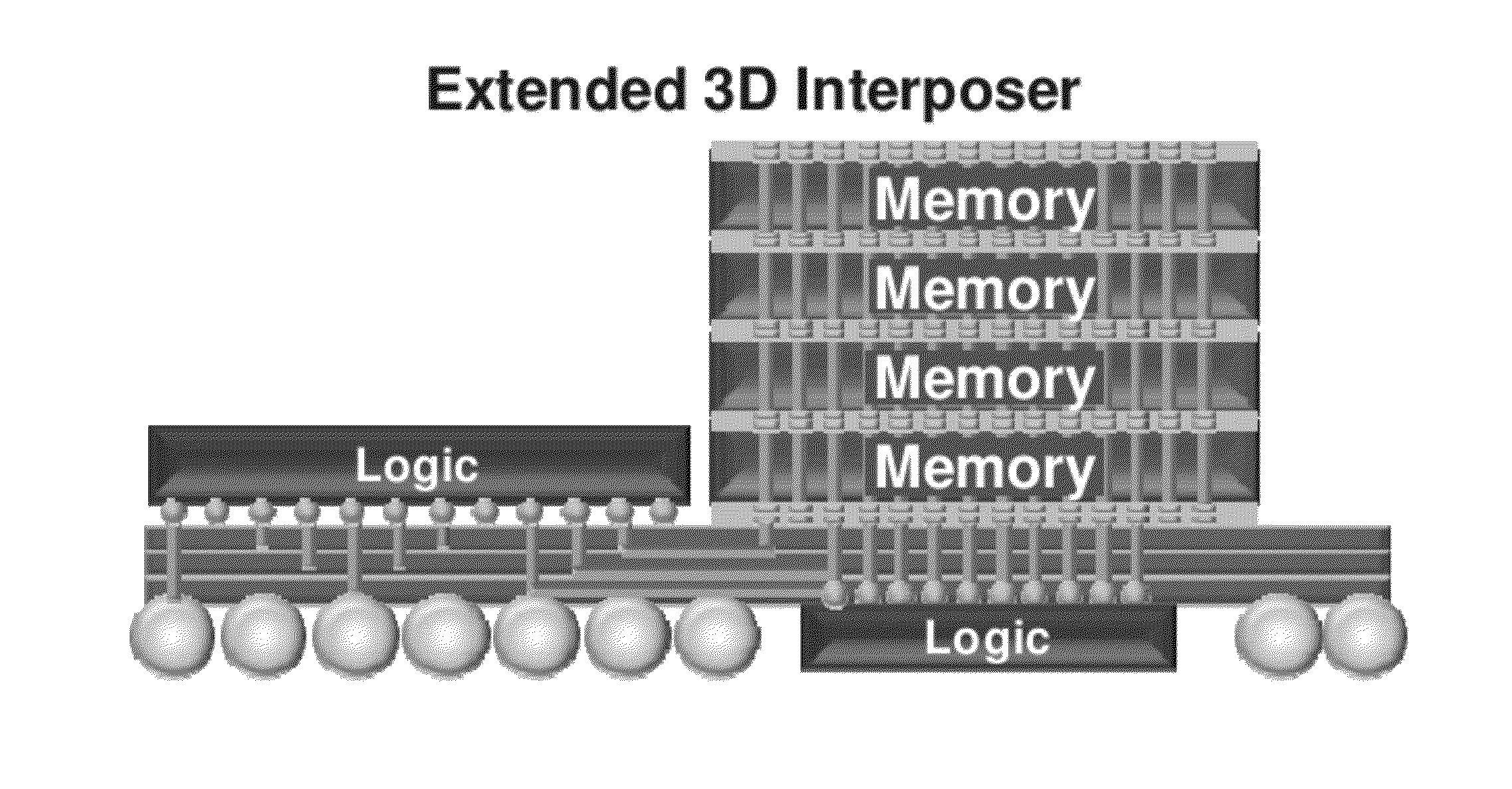
A 3D interconnect structure comprising an ultra-thin interposer having a plurality of ultra-high density of through-via interconnections defined therein. The 3D interposer electrically connects first and second electronic devices in vertical dimension and has the same or similar through-via density as the first or second electronic devices it connects. The various embodiments of the interconnect structure allows 3D ICs to be stacked with or without TSVs and increases bandwidth between the two electronic devices as compared to other interconnect structures of the prior art. Further, the interconnect structure of the present invention is scalable, testable, thermal manageable, and can be manufactured at relatively low costs. Such a 3D structure can be used for a wide variety of applications that require a variety of heterogeneous ICs, such as logic, memory, graphics, power, wireless and sensors that cannot be integrated into single ICs.

Description

CROSS-REFERENCE TO RELATED APPLICATION[0001]This application claims the benefit of U.S. Provisional Patent Application Ser. No. 61 / 409,221, filed 2 Nov. 2010, which is incorporated herein by reference in its entirety as if fully set forth below.BACKGROUND[0002]1. Field[0003]The various embodiments of the present invention relate to ultra-small pitch interconnect structures comprising of ultra-thin interposers having ultra-high density through vias defined therein.[0004]2. Description of Related Art[0005]The increasing number of smart and mobile phone applications, including video streaming, 3D graphics, camera-functions, and gaming, are driving the demand for logic to memory bandwidth (BW) at increasing levels without an increase in power consumption. Bandwidth is defined as bit rate per pin or I / O and the number of I / Os. Bit rate per pin is influenced by many factors, the most important factor being interconnection length between two devices. The main elements that influence bandwi...

Claims


Application Information

Patent Timeline
Patent Type & Authority Applications(United States)
IPC IPC(8): H05K1/18H01L23/498H05K1/11H01L23/48
CPCH01L23/49827H01L25/0652H01L25/0657H01L2225/06517H01L2225/06541H01L2225/06548H01L2924/09701H05K1/141H05K3/3436H05K2201/10378H05K2201/10515H01L21/76898H01L23/3677H01L23/49816H01L23/49822H01L2224/16146H01L2224/16227H01L2224/73204H01L2224/73253H01L2924/15153H01L2924/15311H01L2924/15321H01L2924/19105H01L2225/06565H01L2224/48091H01L2924/00014H01L2924/15192H01L2224/16145H01L2224/16225H01L2224/32145H01L2224/32225H01L2224/48227H01L2224/73265H01L2924/00H01L25/18H01L2225/06589H01L2225/06513H01L2225/06572H01L2224/05573H01L2224/05568H01L2224/05647H01L2224/16235
Inventor SUNDARAM, VENKATESH V.TUMMALA, RAO R.
Owner GEORGIA TECH RES CORP
Learn More