Heat treatment apparatus for heating substrate by irradiating substrate with flashes of light

a technology of heat treatment apparatus and electronic substrate, which is applied in the direction of lighting and heating apparatus, electric heating for furnaces, furnaces, etc., can solve the problems of poor device formation, impaired temperature distribution uniformity in the inner region, and impaired uniformity of temperature distribution in the peripheral portion, so as to simplify the configuration of the heat treatment apparatus

Active Publication Date: 2012-03-22
DAINIPPON SCREEN MTG CO LTD
View PDF1 Cites 28 Cited by
  • Summary
  • Abstract
  • Description
  • Claims
  • Application Information

AI Technical Summary

Benefits of technology

[0015]The heat treatment apparatus includes the halogen lamp which irradiates the substrate held by the holder made of quartz with light from below to preheat the substrate. This eliminates the nonuniformity of the temperature distribution when the local region lower in temperature than other regions is produced by preheating.
[0017]This raises the temperature of the peripheral portion to achieve a uniform in-plane temperature distribution of the substrate, when the temperature of the peripheral portion of the substrate is lower than that of other regions.
[0019]This increases the width of a region irradiated with laser light in the peripheral portion of the substrate.
[0023]This allows the reflected light to precisely reach the local region irradiated with light from the auxiliary irradiation part.
[0025]This makes fine adjustments of the position reached by the reflected light from the reflective part to achieve a uniform in-plane temperature distribution of the substrate with higher accuracy.
[0027]This eliminates the need to provide the space for placement of the purpose-built reflective part, and also simplifies the configuration of the heat treatment apparatus.

Problems solved by technology

This results in a junction depth much greater than a required depth, which might present a problem in good device formation.
When the amount of light directed from the halogen lamps onto the peripheral portion of the wafer for preheating is increased for the purpose of solving the problem of the temperature fall in the peripheral portion, the temperature of part of the peripheral portion rises, as shown in FIG. 27B, but the temperature distribution uniformity in the inner region, rather than in the peripheral portion, is impaired.
Additionally, the temperature fall in an outermost edge portion of the semiconductor wafer still remains unsolved.

Method used


Image

  • Heat treatment apparatus for heating substrate by irradiating substrate with flashes of light
  • Heat treatment apparatus for heating substrate by irradiating substrate with flashes of light
  • Heat treatment apparatus for heating substrate by irradiating substrate with flashes of light

Examples


first preferred embodiment

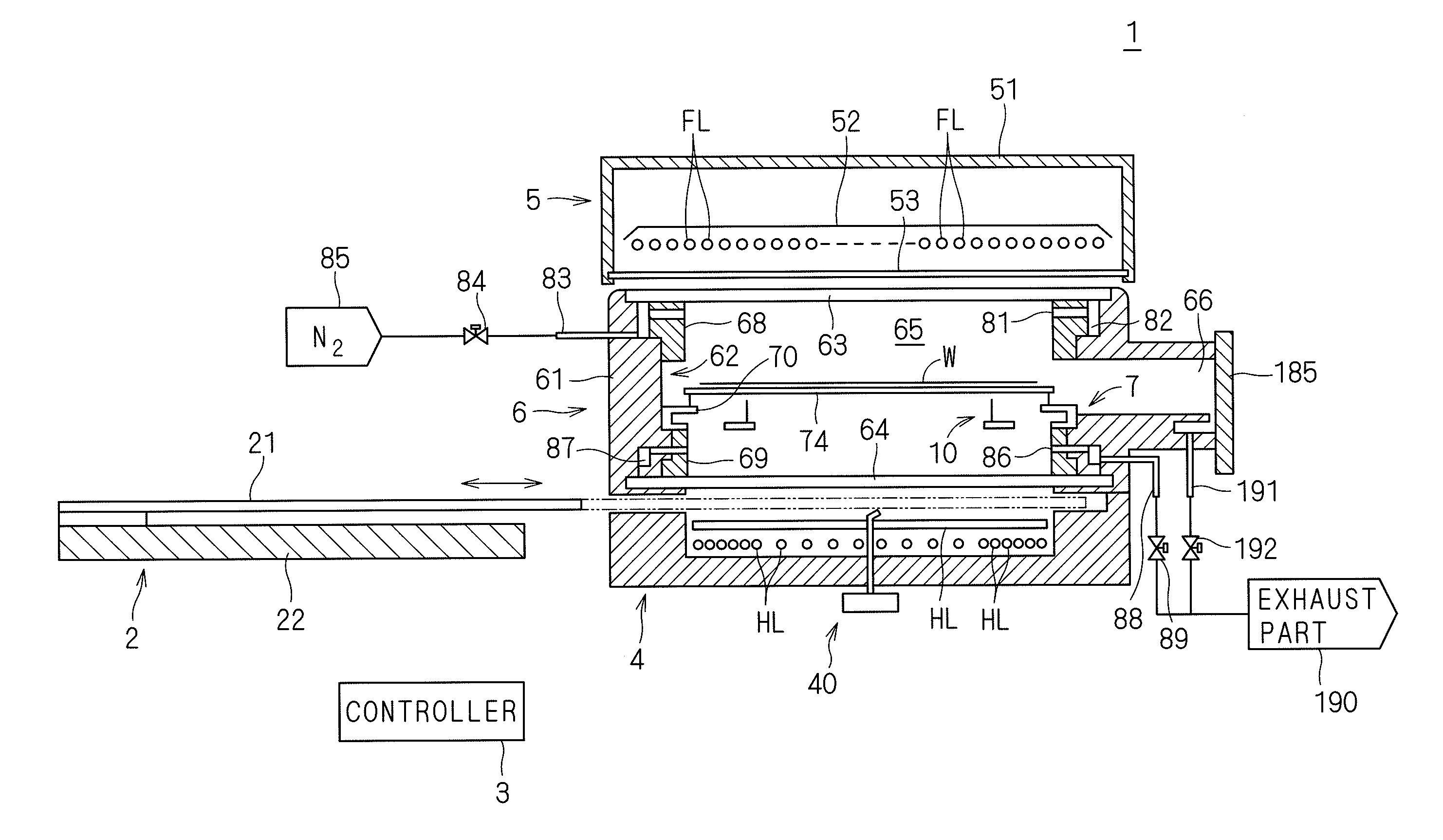
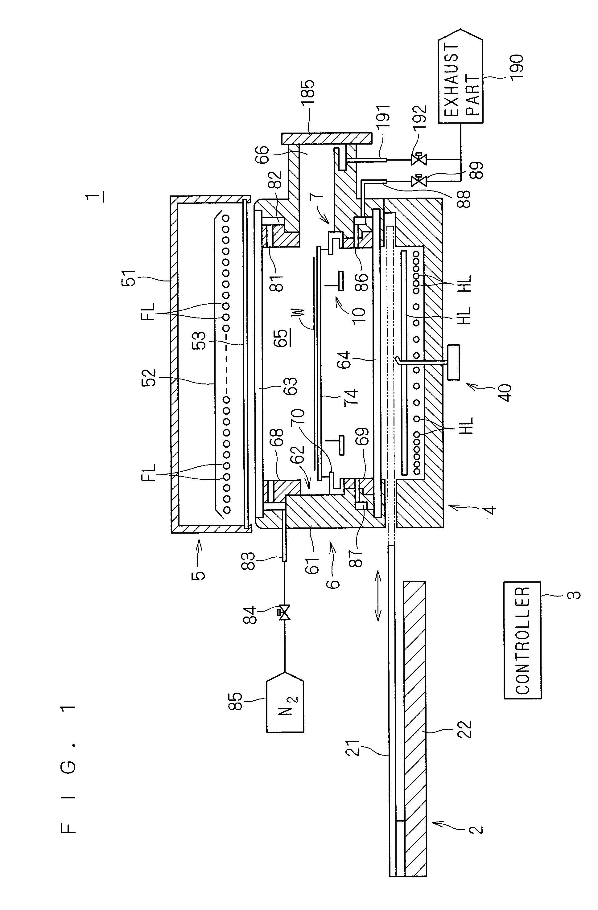
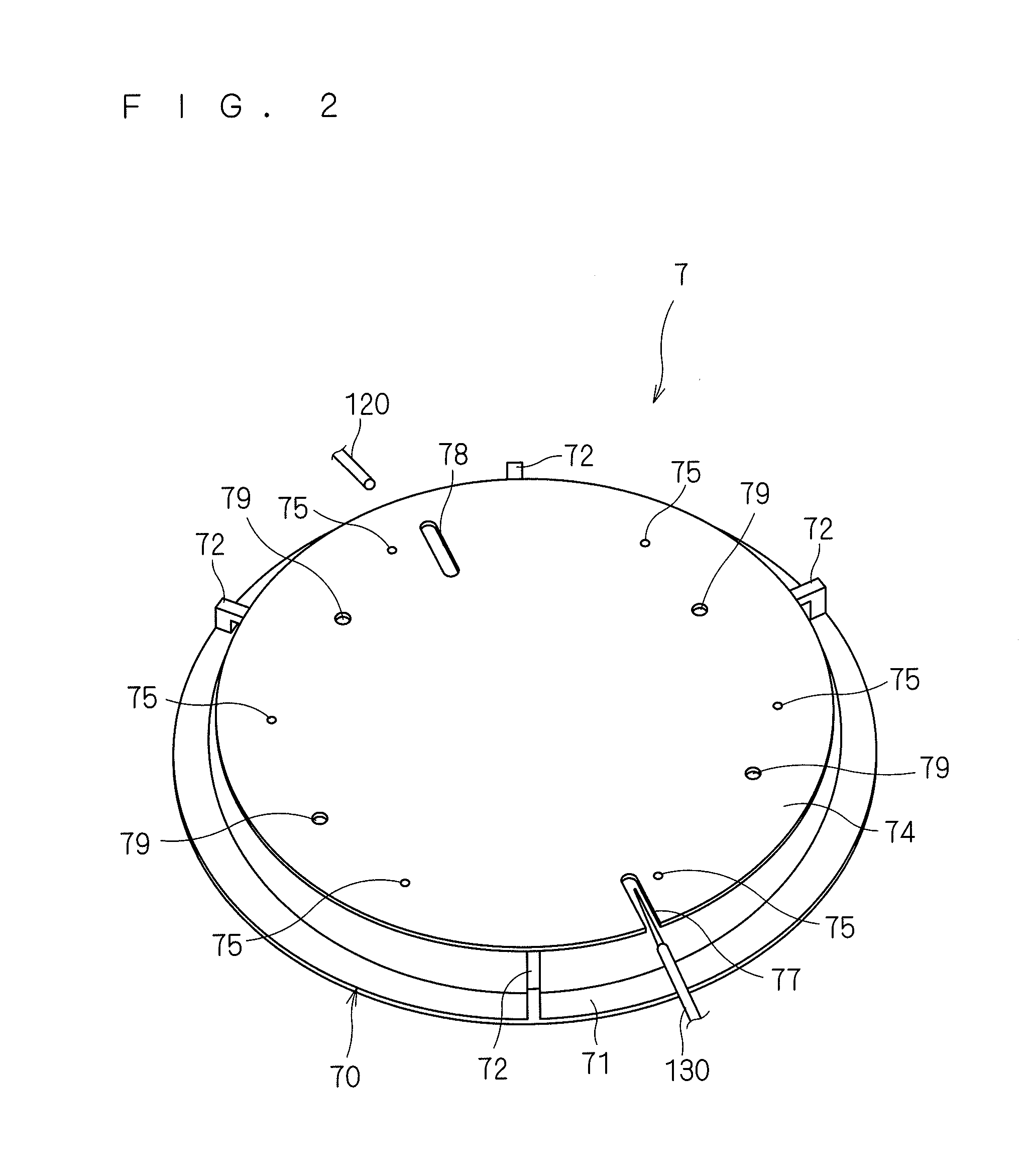
[0058]FIG. 1 is a longitudinal sectional view showing a configuration of a heat treatment apparatus 1 according to a first preferred embodiment of the present invention. The heat treatment apparatus 1 according to the first preferred embodiment is a flash lamp annealer for irradiating a generally disk-shaped semiconductor wafer W having a diameter of 300 mm and serving as a substrate with flashes of light to heat the semiconductor wafer W. A semiconductor wafer W prior to the transport into the heat treatment apparatus 1 is implanted with impurities. The heat treatment apparatus 1 performs a heating treatment on the semiconductor wafer W to thereby activate the impurities implanted in the semiconductor wafer W.

[0059]The heat treatment apparatus 1 includes a chamber 6 for receiving a semiconductor wafer W therein, a flash heating part 5 including a plurality of built-in flash lamps FL, a halogen heating part 4 including a plurality of built-in halogen lamps HL, and a shutter mechanis...

second preferred embodiment

[0124]Next, a second preferred embodiment according to the present invention will be described. FIG. 13 is a view showing a configuration of the auxiliary irradiation part 40 according to the second preferred embodiment. Like reference numerals and characters are used in FIG. 13 to designate components identical with those in FIG. 9. The auxiliary irradiation part 40 according to the second preferred embodiment includes a cam mechanism in addition to the components of the first preferred embodiment. Specifically, the auxiliary irradiation part 40 according to the second preferred embodiment includes a cam-follower 47 fixedly provided on the rotary motor 44, and a cam 46 abutting against the cam-follower 47. The configuration of the heat treatment apparatus 1 according to the second preferred embodiment is similar to that according to the first preferred embodiment except that the auxiliary irradiation part 40 includes the cam mechanism. A procedure for the treatment of a semiconduct...

third preferred embodiment

[0128]Next, a third preferred embodiment according to the present invention will be described. FIG. 15 is a view showing a configuration of the auxiliary irradiation part 40 according to the third preferred embodiment. Like reference numerals and characters are used in FIG. 15 to designate components identical with those in FIG. 9. The auxiliary irradiation part 40 according to the third preferred embodiment includes a galvanometer mirror 49 in place of the laser light emitting part 45 of the first and second preferred embodiments. The galvanometer mirror 49 includes two mirrors individually rotatable through an angle dependent upon a driving voltage to allow incident laser light to scan a two-dimensional surface (in X and Y directions) while reflecting the incident laser light. The configuration of the heat treatment apparatus 1 according to the third preferred embodiment is similar to that according to the first preferred embodiment except that the auxiliary irradiation part 40 in...


PUM


Abstract

When a semiconductor wafer is preheated by halogen lamps, the temperature of a peripheral portion of the semiconductor wafer is lower than that of a central portion thereof. A laser light emitting part disposed immediately under the center of the semiconductor wafer is rotated about the center line of the semiconductor wafer, while laser light is directed from the laser light emitting part toward the peripheral portion of the semiconductor wafer. Thus, the irradiation spot of the laser light exiting the laser light emitting part swirls around along the peripheral portion of the back surface of the semiconductor wafer so as to draw a circular trajectory. As a result, the entire peripheral portion of the semiconductor wafer at a relatively low temperature is uniformly heated. This achieves a uniform in-plane temperature distribution of the semiconductor wafer.

Description

BACKGROUND OF THE INVENTION[0001]1. Field of the Invention[0002]The present invention relates to a heat treatment apparatus for heating a thin plate-like precision electronic substrate such as a semiconductor wafer and a glass substrate for a liquid crystal display device (hereinafter referred to simply as a “substrate”) by irradiating the substrate with flashes of light.[0003]2. Description of the Background Art[0004]In the process of manufacturing a semiconductor device, impurity doping is an essential step for forming a pn junction in a semiconductor wafer. At present, it is common practice to perform impurity doping by an ion implantation process and a subsequent annealing process. The ion implantation process is a technique for causing ions of impurity elements such as boron (B), arsenic (As) and phosphorus (P) to collide against the semiconductor wafer with high acceleration voltage, thereby physically implanting the impurities into the semiconductor wafer. The implanted impur...

Claims


Application Information

Patent Timeline
Patent Type & Authority Applications(United States)
IPC IPC(8): H05B1/00
CPCH01L21/67115
Inventor KUSUDA, TATSUFUMIAOTANI, TOSHIAKIMIYAWAKI, SHINJI
Owner DAINIPPON SCREEN MTG CO LTD
Why Eureka
Try Eureka