Method of making a semiconductor chip assembly with a post/dielectric/post heat spreader

a technology of post-dielectric and post-spreader, which is applied in the manufacture of printed circuits, printed circuit aspects, basic electric elements, etc., can solve the problems of heat not only degrading the chip, short life span and immediate failure of the semiconductor device at high operating temperature, and easy degradation of performance, etc., to achieve excellent heat spreading and heat dissipation, and low cost. , the effect of low thermal conductivity

Inactive Publication Date: 2011-11-24
BRIDGE SEMICON
View PDF8 Cites 10 Cited by
  • Summary
  • Abstract
  • Description
  • Claims
  • Application Information

AI Technical Summary

Benefits of technology

[0044]The dielectric base can cover the first post and the first adhesive in the second vertical direction, cover the second post and the second adhesive in the first vertical direction, support the posts and the adhesives and extend to peripheral edges of the assembly. The dielectric base can also be various thermally conductive, electrically insulative organic or inorganic materials such as epoxy, polyimide and diamond-like carbon (DLC). The dielectric base can also be primarily plastic such as epoxy or polyimide and include a reinforcement such as E-glass to increase strength and a filler such as aluminum oxide or aluminum nitride to increase thermal conductivity. In any case, the dielectric base thermally connects and electrically isolates the posts.
[0092]The present invention has numerous advantages. The heat spreader can provide excellent heat spreading and heat dissipation without heat flow through the adhesives. As a result, the adhesives can be a low cost dielectric with low thermal conductivity and not prone to delamination. The first post can provide thermal expansion matching with a semiconductor device mounted thereon, thereby increasing reliability. The first cap can be customized for the semiconductor device, thereby enhancing the thermal connection. The first adhesive can be sandwiched between the dielectric base and the pad and the second adhesive can be sandwiched between the dielectric base and the terminal, thereby providing a robust mechanical bond between the heat spreader and the conductive trace. The dielectric base can provide electrical isolation that protects the semiconductor device from electrostatic discharge in the second cap and enables the second cap to electrically float during operation of the semiconductor device. The conductive trace can provide signal routing with simple circuitry patterns or flexible multi-layer signal routing with complex circuitry patterns. The electrical interconnect can be a plated through-hole formed after the adhesives are solidified and remain a hollow tube or be split at a peripheral edge of the assembly. As a result, a solder joint subsequently reflowed on the terminal can wet and flow into the plated through-hole without creating a buried void in the solder joint beneath the plated through-hole that might otherwise occur if the plated through-hole is filled with the adhesives or another non-wettable insulator, thereby increasing reliability. The dielectric base can provide mechanical support for the conductive layers, the dielectric layers and the adhesives, thereby preventing warping. The assembly can be manufactured using low temperature processes which reduces stress and improves reliability. The assembly can also be manufactured using well-controlled processes which can be easily implemented by circuit board, lead frame and tape manufacturers.

Problems solved by technology

Semiconductor devices are susceptible to performance degradation as well as short life span and immediate failure at high operating temperatures.
The heat not only degrades the chip, but also imposes thermal stress on the chip and surrounding elements due to thermal expansion mismatch.
LEDs include high power chips that generate high light output and considerable heat.
Unfortunately, LEDs exhibit color shifts and low light output as well as short lifetimes and immediate failure at high operating temperatures.
Furthermore, LED light output and reliability are constrained by heat dissipation limits.
However, since the plastic and the dielectric layer typically have low thermal conductivity, the PBGA provides poor heat dissipation.
However, since the lead frame type interposer has limited routing capability, the QFN package cannot accommodate high input / output (I / O) chips or passive elements.
However, manually dropping the heat slug into the central opening is prohibitively cumbersome and expensive for high volume manufacture.
Furthermore, since the heat slug is difficult to accurately position in the central opening due to tight lateral placement tolerance, voids and inconsistent bond lines arise between the substrate and the heat slug.
The substrate is therefore partially attached to the heat slug, fragile due to inadequate support by the heat slug and prone to delamination.
The heat slug is therefore non-planar and difficult to bond to.
As a result, the assembly suffers from high yield loss, poor reliability and excessive cost.
However, the insulating layer sandwiched between the metal core layer and the PCB limits the heat flow to the PCB.
As a result, the heat spreader releases the heat by thermal convection rather than thermal conduction which severely limits the heat dissipation.
Consequently, the substrate is unbalanced and wobbles and warps during manufacture.
This creates enormous difficulties with chip mounting, wire bonding and encapsulant molding.
Furthermore, the expanded base may be bent by the encapsulant molding and may impede soldering the package to the next level assembly as the solder balls collapse.
As a result, the package suffers from high yield loss, poor reliability and excessive cost.
However, the electrical contacts are difficult to mount on the insulating layer, difficult to electrically connect to the next level assembly and fail to provide multi-layer routing.
Conventional packages and thermal boards thus have major deficiencies.
For instance, dielectrics with low thermal conductivity such as epoxy limit heat dissipation, whereas dielectrics with higher thermal conductivity such as epoxy filled with ceramic or silicon carbide have low adhesion and are prohibitively expensive for high volume manufacture.
The dielectric may delaminate during manufacture or prematurely during operation due to the heat.
The substrate may have single layer circuitry with limited routing capability or multi-layer circuitry with thick dielectric layers which reduce heat dissipation.
The heat spreader may be inefficient, cumbersome or difficult to thermally connect to the next level assembly.
The manufacturing process may be unsuitable for low cost, high volume manufacture.

Method used


Image

  • Method of making a semiconductor chip assembly with a post/dielectric/post heat spreader
  • Method of making a semiconductor chip assembly with a post/dielectric/post heat spreader
  • Method of making a semiconductor chip assembly with a post/dielectric/post heat spreader

Examples


Embodiment Construction

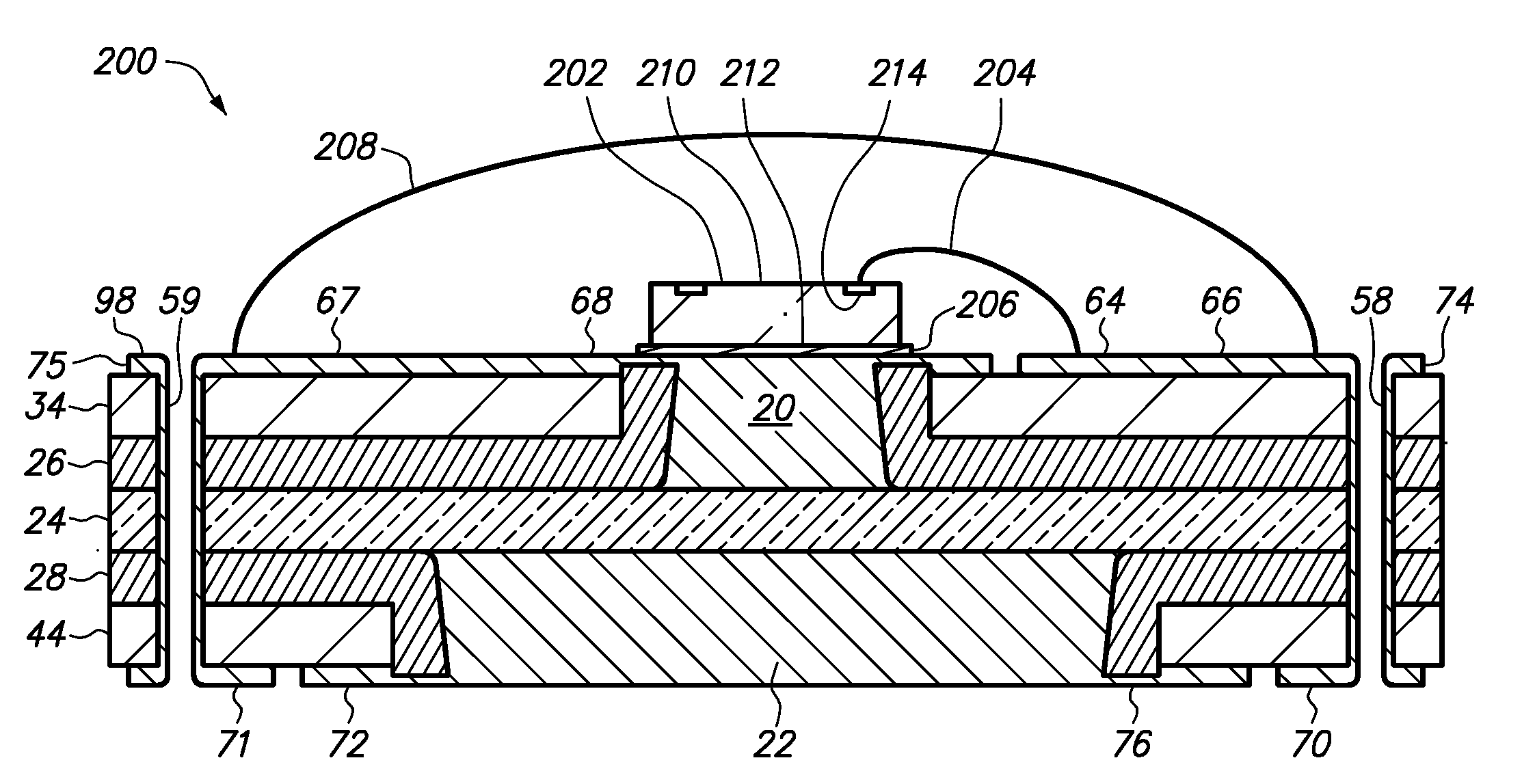
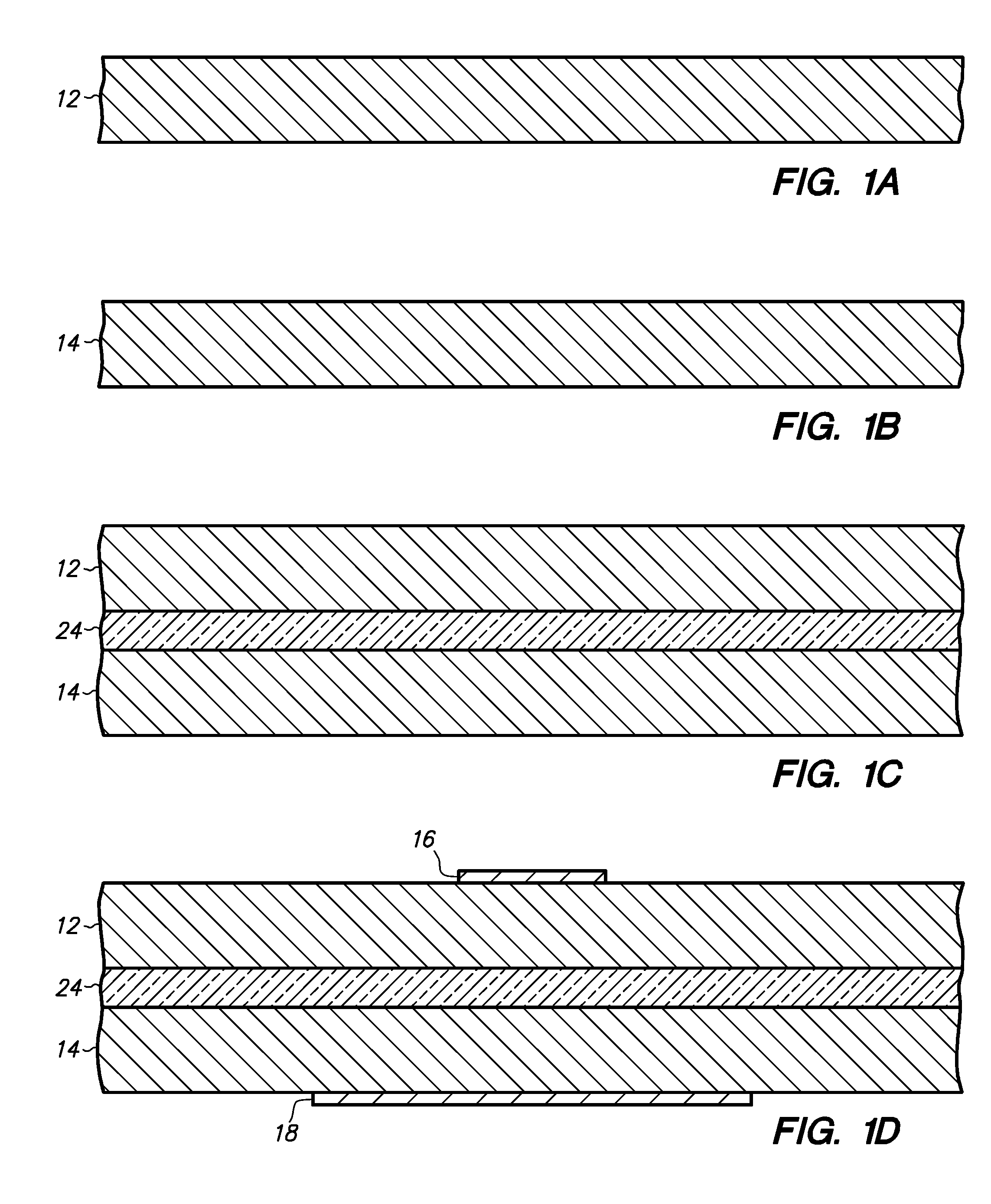
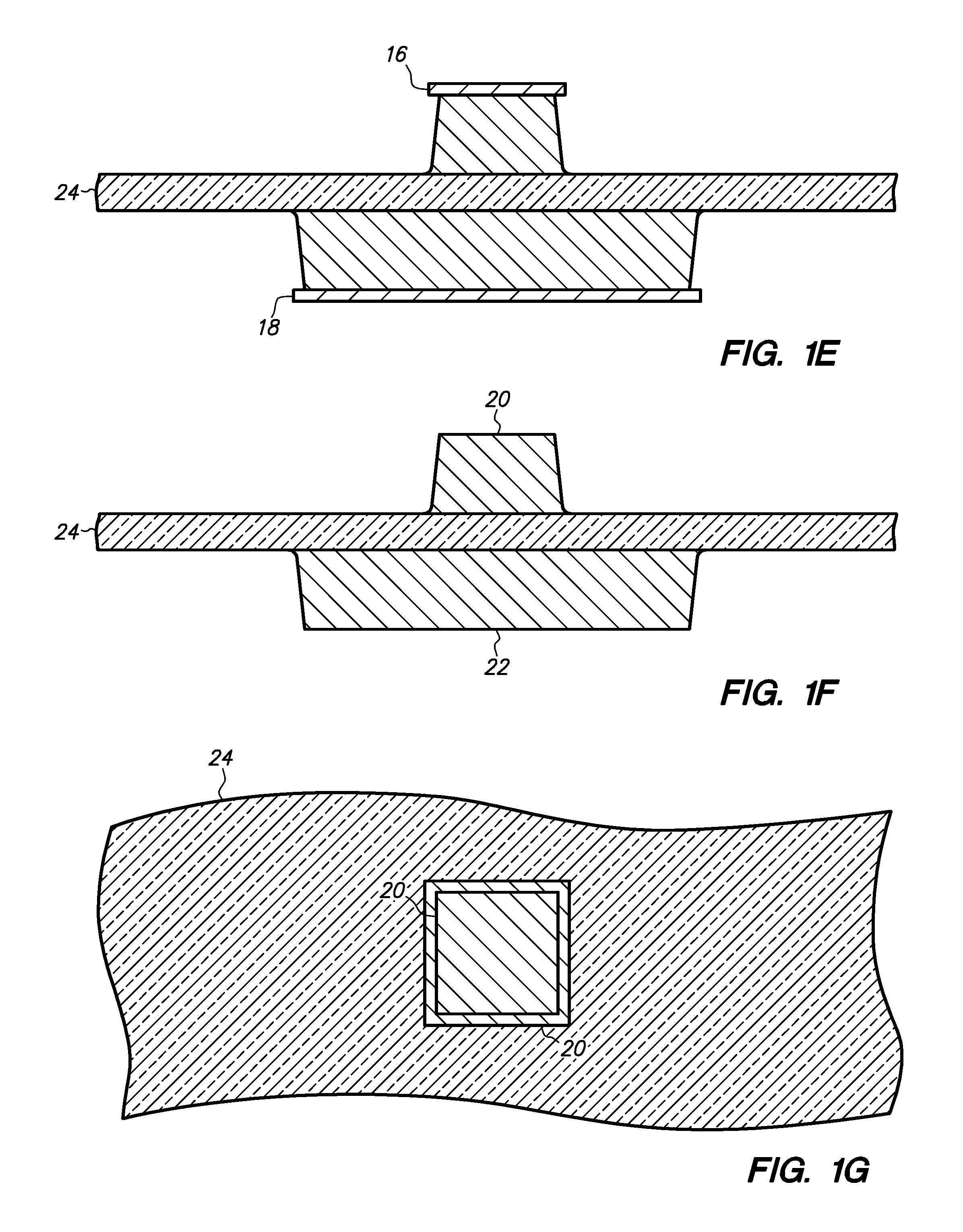
[0113]FIGS. 1A-1F are cross-sectional views showing a method of making first and second posts and a dielectric base in accordance with an embodiment of the present invention, and FIGS. 1G and 1H are top and bottom views, respectively, corresponding to FIG. 1F.

[0114]FIG. 1A. is a cross-sectional view of metal plate 12 which includes opposing major lateral surfaces that face in opposite vertical directions. Metal plate 12 is illustrated as a copper plate with a thickness of 200 microns. Copper has high thermal conductivity, good bondability and low cost. Metal plate 12 can be various metals such as copper, aluminum, alloy 42, iron, nickel, silver, gold, combinations thereof, and alloys thereof.

[0115]FIG. 1B is a cross-sectional view of metal plate 14. For instance, metal plate 14 is a copper plate with a thickness of 200 microns that is identical to metal plate 12.

[0116]FIG. 1C. is a cross-sectional view of metal plates 12 and 14 and dielectric base 24.

[0117]Dielectric base 24 is an e...


PUM


Abstract

A method of making a semiconductor chip assembly includes providing first and second posts, first and second adhesives, first and second conductive layers and a dielectric base, wherein the first post extends from the dielectric base in a first vertical direction into a first opening in the first adhesive and is aligned with a first aperture in the first conductive layer, the second post extends from the dielectric base in a second vertical direction into a second opening in the second adhesive and is aligned with a second aperture in the second conductive layer and the dielectric base is sandwiched between and extends laterally from the posts, then flowing the first adhesive in the first vertical direction and the second adhesive in the second vertical direction, solidifying the adhesives, then providing a conductive trace that includes a pad, a terminal and selected portions of the conductive layers, wherein the pad extends beyond the dielectric base in the first vertical direction and the terminal extends beyond the dielectric base in the second vertical direction, providing a heat spreader that includes the posts and the dielectric base, then mounting a semiconductor device on the first post, electrically connecting the semiconductor device to the conductive trace and thermally connecting the semiconductor device to the heat spreader.

Description

CROSS-REFERENCE TO RELATED APPLICATIONS[0001]This application is a continuation-in-part of U.S. application Ser. No. 12 / 616,773 filed Nov. 11, 2009 and a continuation-in-part of U.S. application Ser. No. 12 / 616,775 filed Nov. 11, 2009, each of which is incorporated by reference. This application also claims the benefit of U.S. Provisional Application Ser. No. 61 / 481,733 filed May 3, 2011, which is incorporated by reference.[0002]U.S. application Ser. No. 12 / 616,773 filed Nov. 11, 2009 and U.S. application Ser. No. 12 / 616,775 filed Nov. 11, 2009 are each a continuation-in-part of U.S. application Ser. No. 12 / 557,540 filed Sep. 11, 2009 and a continuation-in-part of U.S. application Ser. No. 12 / 557,541 filed Sep. 11, 2009.[0003]U.S. application Ser. No. 12 / 557,540 filed Sep. 11, 2009 and U.S. application Ser. No. 12 / 557,541 filed Sep. 11, 2009 are each a continuation-in-part of U.S. application Ser. No. 12 / 406,510 filed Mar. 18, 2009, which claims the benefit of U.S. Provisional Appli...

Claims


Application Information

Patent Timeline
Patent Type & Authority Applications(United States)
IPC IPC(8): H01L33/62H01L21/58
CPCH01L21/486H01L23/3677H01L24/29H01L24/32H01L24/45H01L24/48H01L24/83H01L24/85H01L33/483H01L33/642H01L2224/2919H01L2224/29339H01L2224/32188H01L2224/32225H01L2224/45144H01L2224/48091H01L2224/48106H01L2224/48227H01L2224/73265H01L2224/83855H01L2224/85207H01L2224/85439H01L2224/92H01L2224/92247H01L2924/01012H01L2924/01014H01L2924/01046H01L2924/0105H01L2924/01058H01L2924/01077H01L2924/01078H01L2924/01079H01L2924/19041H05K1/0204H05K3/0061H05K2201/09054H05K2201/10106H05K2203/0369H01L2924/0132H01L2924/01019H01L2924/01087H01L2924/01322H01L2924/014H01L2924/0134H01L2224/29111H01L2224/2929H01L2924/01013H01L2924/01028H01L2924/01029H01L2924/12041H01L2924/00014H01L2924/0665H01L2924/01007H01L2924/01031H01L2924/01015H01L2924/01047H01L2924/01026H01L2924/0104H01L2924/01033H01L2924/00H01L2924/351H01L2224/48639H01L2924/181H01L2924/00012
Inventor LIN, CHARLES W.C.WANG, CHIA-CHUNG
Owner BRIDGE SEMICON
Why Eureka
Try Eureka