Surface light source element and image display including the same
a technology of image display and which is applied in the direction of lighting and heating apparatus, lighting device details, instruments, etc., can solve the problems of insufficient performance and image display still does not have the required brightness, so as to improve the front direction brightness of surface light source element, reduce the thickness of light-guiding plate, and high incident efficiency of light
- Summary
- Abstract
- Description
- Claims
- Application Information
AI Technical Summary
Benefits of technology
Problems solved by technology
Method used
Image
Examples
embodiment 1
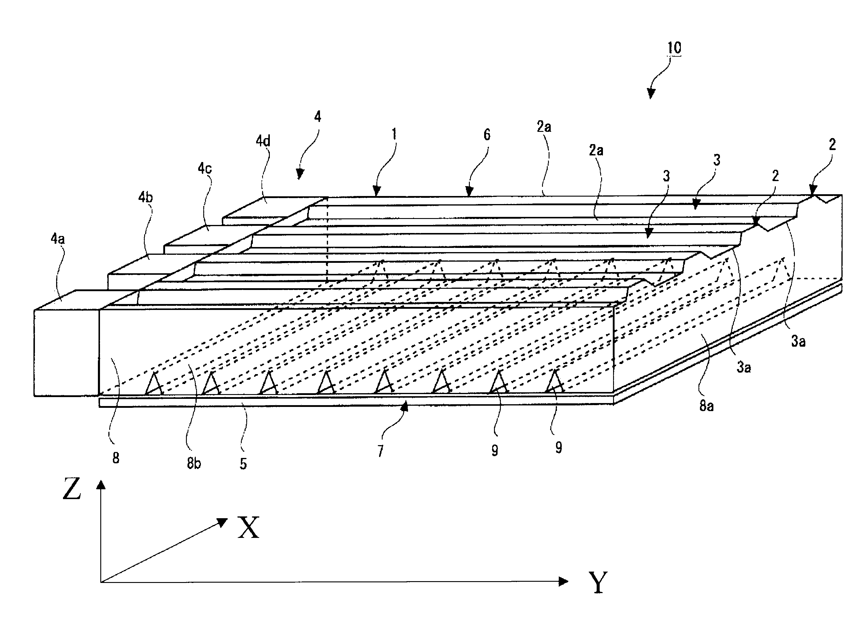
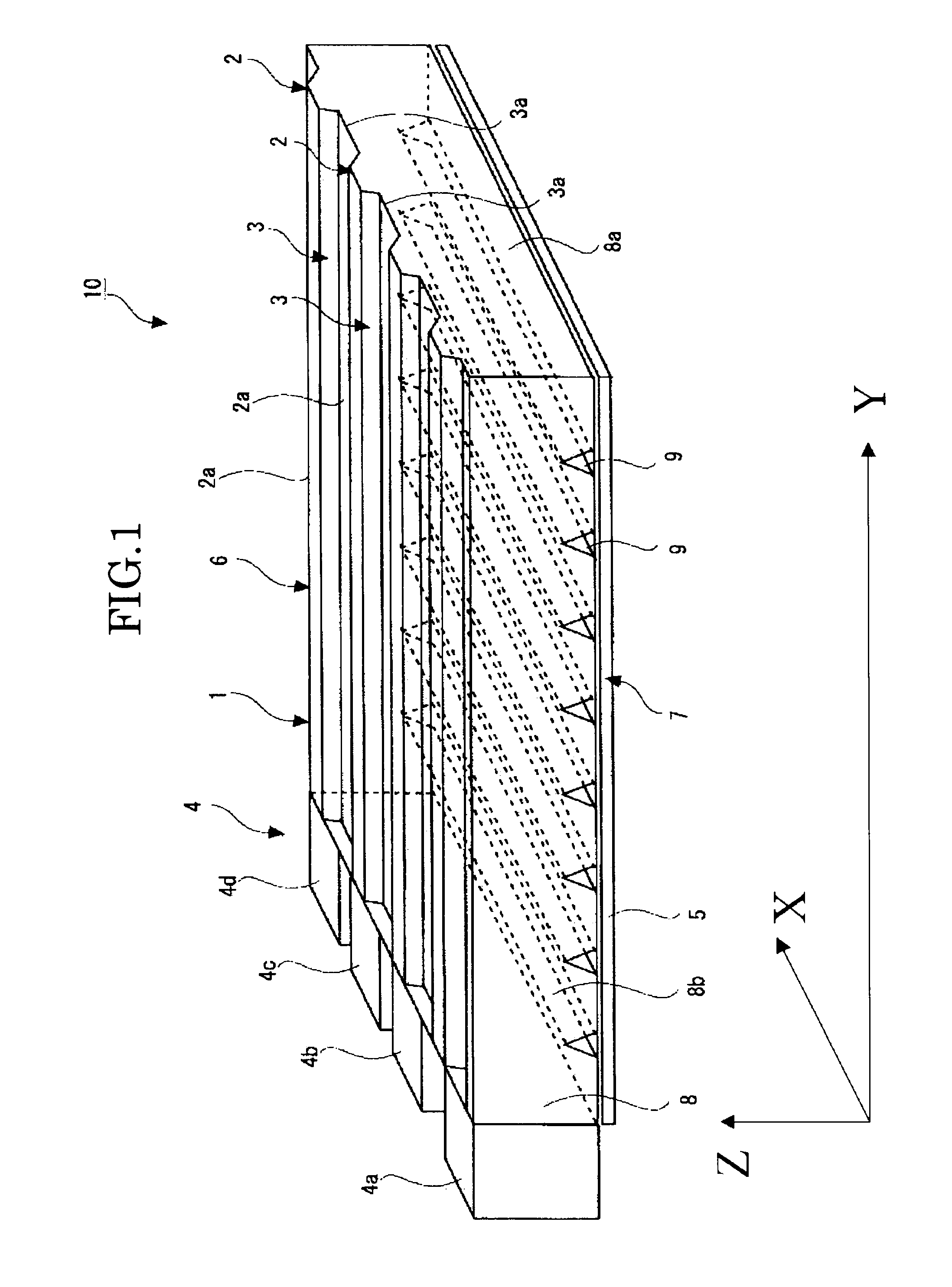
[0130]A mirror stamper made of SUS was used for forming a stamper (hereinafter referred to as stamper 1) on the exit surface side. On the other hand, a stamper (hereinafter referred to as stamper 2) on the bottom surface side, in which prism patterns each having 0.007 mm in height and 130° in top angle were arranged at predetermined intervals, was manufactured by directly forming V-shaped concave stripes each having 0.007 mm in height and 130° in top angle in a mold insert by a cutting process using a diamond bit, forming a nickel electroformed layer by performing direct electroforming from the cut insert, and removing the master.
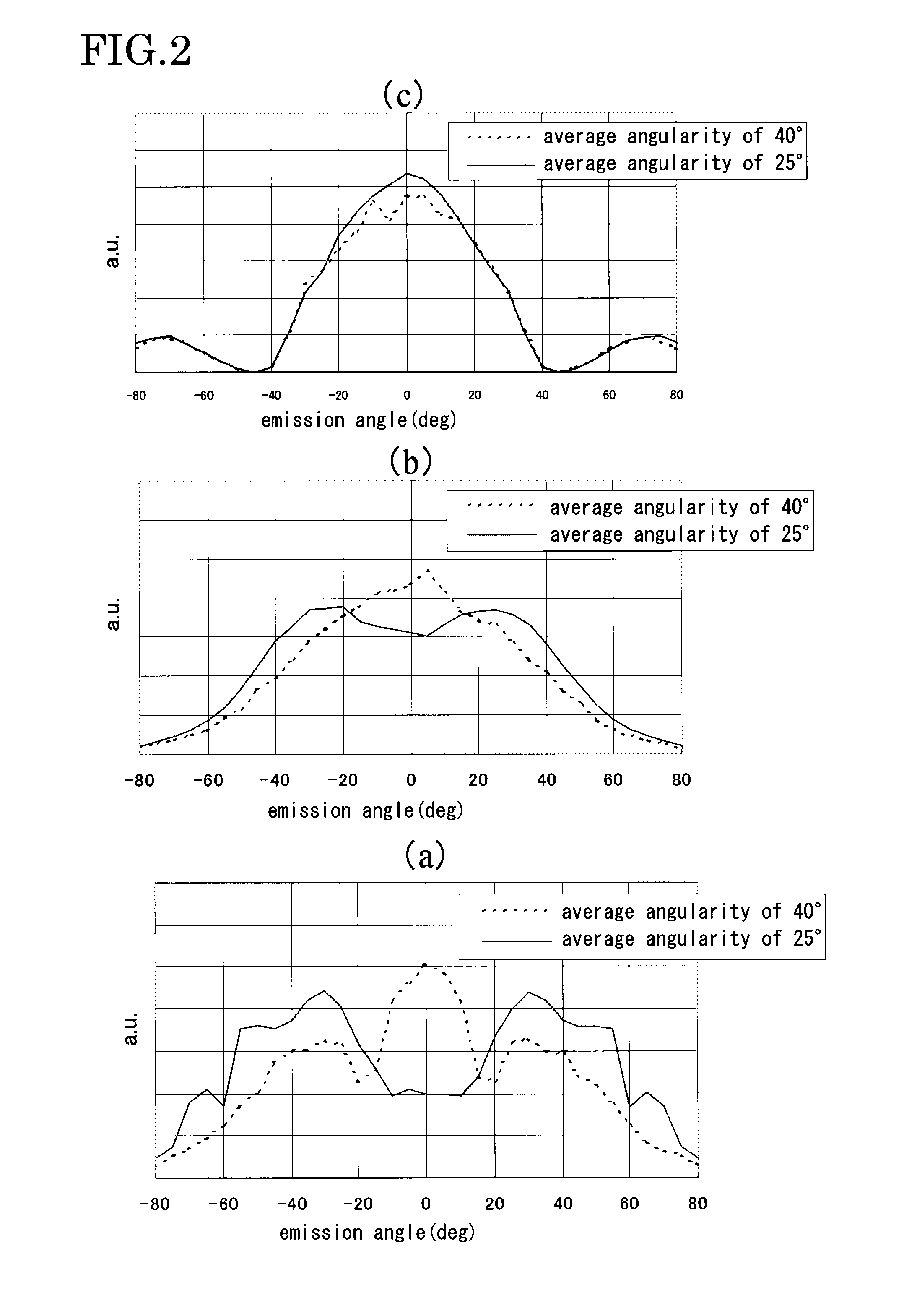
[0131]As molds for transferring, the stampers 1, 2 were assembled in a mold stationary side cavity and a mold movable side cavity of an injection machine, and a light-guiding plate having a fine structure for a 40 inch-liquid crystal television was obtained by use of an injection molding process. The obtained light-guiding plate was formed to have the outsi...
embodiment 2
[0136]A negative type photoresist (CA3000) made by Tokyo Ohka Kogyo Co., Ltd. was applied to a cleaning glass, heated for 2 minutes by a hotplate of 110° C. and thereafter cooled to a room temperature. A photomask in which slits were provided at predetermined intervals was closely fitted to the glass substrate, rotated at a constant speed from −35° to +35° and during the rotation, UV light, 1400 mj was irradiated. After the photomask was removed, the substrate was developed. A nickel conductive film was applied to a surface of the obtained master by use of an ordinary method, and a nickel electroformed layer was formed by electroforming nickel as an electroforming metal on the nickel conducted film. In addition, a stamper (hereinafter referred to as stamper 3) on the exit surface side having trapezoidal patterns having 0.01 mm in height, a flat portion having about 0.01 mm in width on the top portion and 55° in inclined angle was made by removing the master from the nickel conducted...
embodiment 3
[0140]A stamper (hereinafter referred to as stamper 5) on the bottom surface side, in which prism patterns each having 0.007 mm in height and 120° in top angle were arranged at predetermined intervals, was made by forming V-shaped concave stripes each having the top angle of 120° and the height of 0.007 mm in a mold insert directly by use of a diamond bit through a cutting process, performing direct electroforming from the mold insert to form a nickel electroformed layer, and removing the master.
[0141]As molds for transferring, the stampers 3, 5 were assembled in a mold-stationary side cavity and a mold-movable side cavity of an injection machine, and a light-guiding plate for a 40 inch-liquid crystal television, having a fine structure was acquired through an injection forming process. The outside size of the obtained light-guiding plate was formed to have 900 mm×511 mm×4 mm in width, length and height, respectively. The obtained light-guiding plate was formed to have a mirror exit...
PUM
 Abstract
Description
Claims
Application Information
 - R&D
- Intellectual Property
- Life Sciences
- Materials
- Tech Scout
- Unparalleled Data Quality
- Higher Quality Content
- 60% Fewer Hallucinations
Browse by: Latest US Patents, China's latest patents, Technical Efficacy Thesaurus, Application Domain, Technology Topic, Popular Technical Reports.
© 2025 PatSnap. All rights reserved.Legal|Privacy policy|Modern Slavery Act Transparency Statement|Sitemap|About US| Contact US: help@patsnap.com


