
Display device, copper alloy film for use therein, and copper alloy sputtering target

a technology of copper alloy film and display device, which is applied in the direction of semiconductor/solid-state device details, instruments, transportation and packaging, etc., can solve the problems of/or insulating film, poor adhesion to glass substrate, and suffer from peeling off from glass substrate, etc., to achieve low electric resistance, large screen size, and high frequency

Inactive Publication Date: 2011-06-23
KOBE STEEL LTD
View PDF49 Cites 19 Cited by
  • Summary
  • Abstract
  • Description
  • Claims
  • Application Information

AI Technical Summary

Benefits of technology

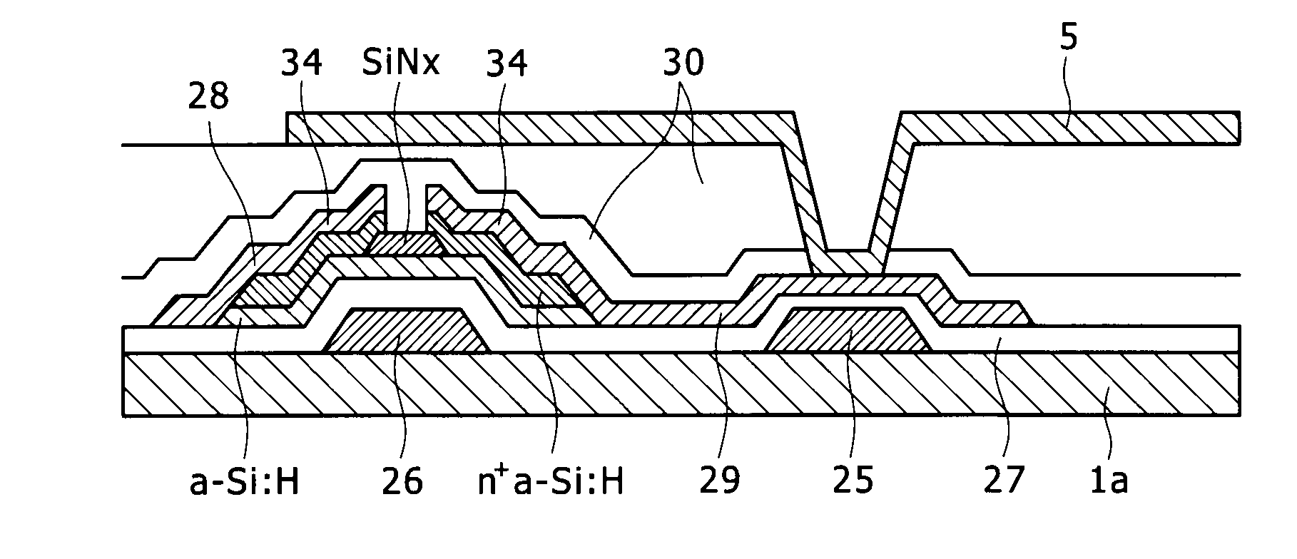
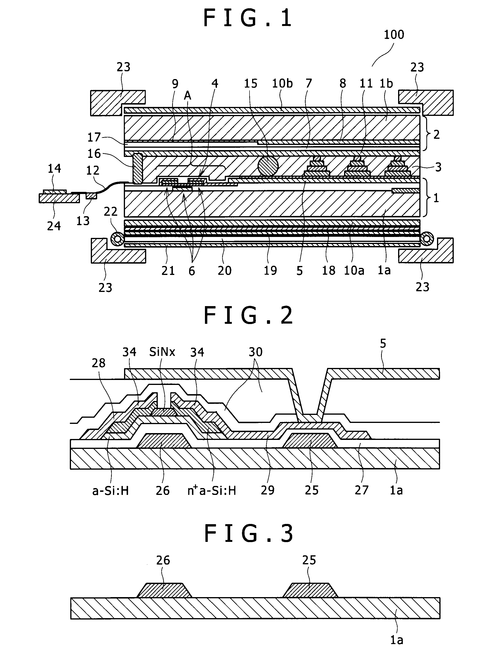
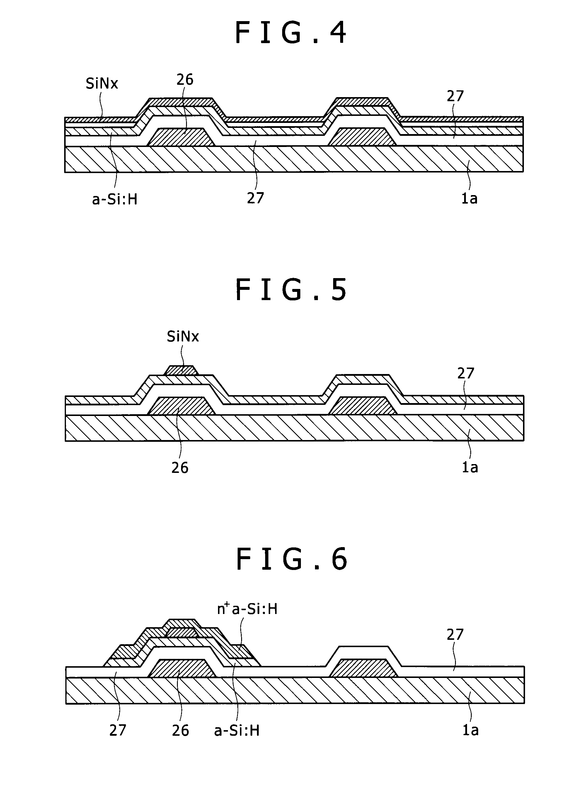
The present invention relates to a display device and a Cu alloy film used in the display device. The technical effects of the invention include improved image quality, high-speed animation, and reduced power consumption. The invention also includes a method for manufacturing the display device using a sputtering target for deposition of the Cu alloy film. The display device includes a TFT array substrate and a counter substrate, with a liquid crystal layer in between. The TFT array substrate has a scanning line and a signal line arranged on it, and a pixel electrode formed from a transparent conductive film. The counter substrate has a common electrode and a light shielding film. The invention also includes a backlight, a spacer, a sealant, a protective film, a diffuser panel, a prism sheet, a light guide panel, a reflector plate, a holding frame, and a printed circuit board.

Problems solved by technology

However, such Cu-based materials, when adopted to interconnections, have poor adhesion to a glass substrate and / or insulating film as compared to the Al-based materials.
An electrode / interconnection composed of a Cu-based material (hereinafter referred to as a “Cu-based electrode / interconnection” or “Cu-based interconnection”) has poor adhesion to the glass substrate and often suffers from peeling off from the glass substrate.
These bilayer structure interconnections, however, require complicated processes and suffer from increased process cost.
In addition, they also suffer from high interconnection resistance as the whole bilayer structure (effective interconnection resistance), because they include the Mo-containing underlayer having a high electric resistance as the interconnection underlayer.
Specifically, as Cr and Mo have electric resistivities higher than that of Cu (Cr has an electric resistivity of 12.9×10⁻⁶ Ω·cm; and Mo has an electric resistivity of 10.0×10⁻⁶Ω·cm), the bilayer interconnections including the Cu-based interconnection and the high-melting-point metal layer suffer from problems of signal delay and power loss caused by high interconnection electric resistances.
In addition, the bilayer interconnections may suffer from corrosion at the interface between Cu and the high-melting-point metal during wet etching using a chemical bath (liquid chemical), because metals of different types, i.e., Cu and the high-melting-point metal (such as Mo) are laminated.
The lamination of the thin films of different materials impedes taper control through wet etching in pattering to form the interconnection.
Specifically, typically when the underlayer in the bilayer structure is etched at a rate higher than that of the upper layer, the underlayer is necked to generate an undercut, and this can impede the formation of the interconnection having a desired profile (cross section) (e.g., a profile with a taper angle of about 45 degrees to about 60 degrees).
According to this technique, however, the resin film may deteriorate to have insufficient adhesion during a high-temperature annealing process in the production of a display device (such as a liquid crystal display panel).

Method used


Image

  • Display device, copper alloy film for use therein, and copper alloy sputtering target
  • Display device, copper alloy film for use therein, and copper alloy sputtering target
  • Display device, copper alloy film for use therein, and copper alloy sputtering target

Examples


example 1

[0138]To evaluate adhesion between a Cu alloy film and a glass substrate, peel tests using an adhesive tape were performed in the following method.

[0139](Preparation of Specimens)

[0140]Initially, a pure Cu film, a pure Mo film, and a series of Cu alloy films having the compositions given in Table 1 were deposited to a thickness of 300 nm on a glass substrate (Eagle 2000 supplied by Corning Inc., having a diameter of 100 mm and a thickness of 0.7 mm) through DC magnetron sputtering under film deposition conditions as mentioned below at room temperature. After deposition, the films were subjected to a heat treatment of holding at 350° C. in a vacuum atmosphere for 30 minutes and thereby yielded adhesion evaluation specimens.

[0141]The pure Cu film and the pure Mo film were deposited using a pure Cu sputtering target and a pure Mo sputtering target, respectively. The Cu alloy films having different compositions were deposited each using, as a sputtering target, a pure Cu sputtering targ...

example 2

[0154]A series of Cu—X-containing alloy films was deposited, and how the adhesion to a glass substrate (the film adhesion rate) varies depending on a heat treatment performed after film deposition was determined.

[0155](Preparation of Specimens)

[0156]A series of Cu—X-containing alloy films (X is Al, Mg or Ti, the X content is 0.1 atomic percent, 2.0 atomic percent or 5.0 atomic percent) was deposited to a thickness of 300 nm on a glass substrate (Eagle 2000 supplied by Corning Inc., having a diameter of 100 mm and a thickness of 0.7 mm) through DC magnetron sputtering by the procedure of Example 1. Next, the following specimens were prepared:

(A) specimens as prepared in the above method (specimens in an as-deposited state),

(B) specimens after subjected to a heat treatment of holding at 350° C. in a vacuum atmosphere for 30 minutes,

(C) specimens after subjected to a heat treatment of holding at 400° C. in a vacuum atmosphere for 30 minutes, and

(D) specimens after subjected to a heat t...

example 3

[0160]A series of Cu—X-containing alloy films was deposited, and the electric resistivities of the alloy films were measured and evaluated.

[0161](Preparation of Specimens)

[0162]A series of Cu—X-containing alloy films (X is Al, Mg or Ti, the X content is 0.1 atomic percent, 2.0 atomic percent or 5.0 atomic percent) was deposited to a thickness of 300 nm on a glass substrate (Eagle 2000 supplied by Corning Inc., having a diameter of 100 mm and a thickness of 0.7 mm) through DC magnetron sputtering by the procedure of Example 1.

[0163](Measurement of Electric Resistivity)

[0164]The above-prepared Cu—X-containing alloy films were processed into stripe patterns (electric resistivity testing patterns) having a width of 100 μm and a length of 10 mm through photolithography and wet etching, and the electric resistivities of the patterns were measured at room temperature by a direct-current four-point probe method using a prober.

[0165]The measurements of the electric resistivities were respect...


PUM

PropertyMeasurementUnit
thicknessaaaaaaaaaa
thicknessaaaaaaaaaa
sizeaaaaaaaaaa

Abstract

Disclosed is a Cu alloy film for a display device that has high adhesion to a glass substrate while maintaining a low electric resistance characteristic of Cu-based materials. The Cu alloy film is wiring in direct contact with a glass substrate on a board and contains 0.1 to 10.0 atomic % in total of one or more elements selected from the group consisting of Ti, Al, and Mg. Also disclosed is a display device comprising a thin-film transistor that comprises the Cu alloy film. In a preferred embodiment of the display device, the thin-film transistor has a bottom gate-type structure, and a gate electrode and scanning lines in the thin-film transistor comprise the Cu alloy film and are in direct contact with the glass substrate.

Description

TECHNICAL FIELD[0001]The present invention relates to a display device and a Cu alloy film for use in the display device. Specifically, the present invention relates to a Cu alloy film constituting an interconnection to be in direct contact with a glass substrate of a thin film transistor (hereinafter also referred to as a “TFT”) of such a display device; to a flat panel display (display device) such as a liquid crystal display or organic electroluminescent (EL) display, which includes the Cu alloy film used in the thin film transistor; and to a sputtering target for the deposition of the Cu alloy film. Of such display devices, the following description is made by taking liquid crystal displays as examples. It should be noted, however, that these examples are never intended to limit the scope of the present invention.BACKGROUND ART[0002]Typically, liquid crystal displays are used in a wide variety of applications ranging from small-sized mobile phones to wide-screen television sets ...

Claims


Application Information

Patent Timeline
Patent Type & Authority Applications(United States)
IPC IPC(8): H01L29/04B32B17/06
CPCC22C9/00C22C9/01H01L23/53233Y10T428/265H01L2924/0002H01L27/124H01L2924/00C23C14/14C23C14/34
Inventor ONISHI, TAKASHIMIKI, AYAGOTO, HIROSHIMIZUNO, MASAOITO, HIROTAKATOMIHISA, KATSUFUMI
Owner KOBE STEEL LTD
Learn More