Electrode of biosensor, manufacturing method thereof, and biosensor thereof
a biosensor and electrode technology, applied in the direction of superimposed coating process, resistive material coating, liquid/solution decomposition chemical coating, etc., can solve the problems of increasing the coefficient of variation (cv), increasing production costs, and increasing production quality, so as to reduce defective rate, increase production quality, and cost
- Summary
- Abstract
- Description
- Claims
- Application Information
AI Technical Summary
Benefits of technology
Problems solved by technology
Method used
Image

Examples
first embodiment
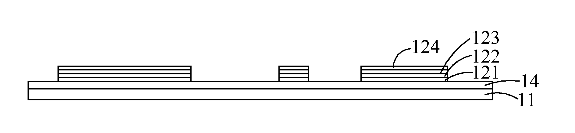
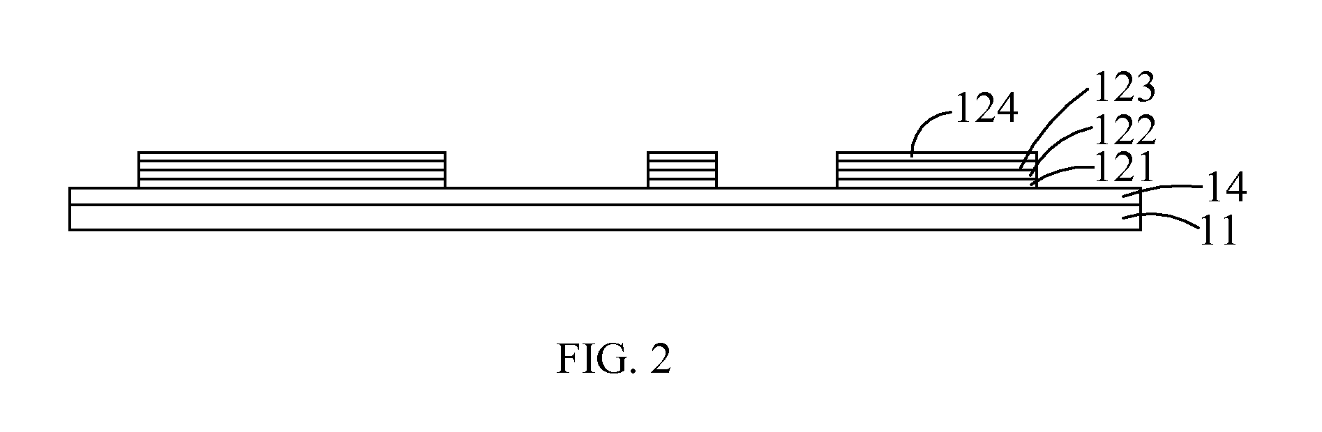
[0038]Please refer to FIG. 4 that is a flowchart illustrating a manufacturing method of an electrode of a biosensor according to the present invention. The steps comprise the follows. In the step S21, a flexible insulation layer is provided. In the step S22, a resin layer is disposed on the surface of the flexible insulation. In the step S23, a first metal layer on the surface of the resin layer. In the step S24, a circuit is etched on the first metal layer via a microetching procedure. In the step S25; a second metal layer, a third metal layer and a fourth metal layer are sequentially disposed on the first metal layer comprising the circuit. The material of the first metal layer comprises copper foil, brass, tombac, phosphorous copper, silver or a combination thereof. The tombac may be an alloy of copper and zinc. The material of the second metal layer comprises palladium. The material of the third metal layer comprises nickel, and the material of the fourth metal layer comprises g...
third embodiment
[0040]Please refer to FIG. 7, a flowchart illustrating a manufacturing method of an electrode according to the present invention is shown. The steps of the manufacturing method comprise the follows. In the step S30, a resin layer is attached on a flexible insulation layer. In the step S31, a copper foil layer is attached on the surface of the resin layer. In the step S32, a light-sensitive film, which is a photoresist comprising circuit patterns to be wanted, is attached on the copper foil layer. In the step S33, an exposure process is preformed on the copper foil layer including the light-sensitive film. In the step S34, circuit patterns are developed on the copper foil layer by a developing machine. In the step S35, the flexible insulation layer including the circuit patterns is immersed into etching liquids to perform an etching process. In the step S36, the flexible insulation layer including the circuit patterns is washed. In the step S37, via an immersion gold process, palladi...
PUM
| Property | Measurement | Unit |
|---|---|---|
| Thickness | aaaaa | aaaaa |
| Thickness | aaaaa | aaaaa |
| Flexibility | aaaaa | aaaaa |
Abstract
Description
Claims
Application Information
 - R&D
- Intellectual Property
- Life Sciences
- Materials
- Tech Scout
- Unparalleled Data Quality
- Higher Quality Content
- 60% Fewer Hallucinations
Browse by: Latest US Patents, China's latest patents, Technical Efficacy Thesaurus, Application Domain, Technology Topic, Popular Technical Reports.
© 2025 PatSnap. All rights reserved.Legal|Privacy policy|Modern Slavery Act Transparency Statement|Sitemap|About US| Contact US: help@patsnap.com