
Gate of a transistor and method of forming the same

a transistor and gate technology, applied in the field of gate of a transistor, can solve the problems of increasing electric power consumption, buried channel type pmos transistor including polysilicon doped with n-type impurities, and may not meet the required characteristics of a semiconductor device, and achieve the effect of improving threshold voltage distribution, excellent surface morphology, and reducing threshold voltage of a pmos transistor

Inactive Publication Date: 2011-02-24
KIM JIN GYUN +2
View PDF8 Cites 0 Cited by
  • Summary
  • Abstract
  • Description
  • Claims
  • Application Information

AI Technical Summary

Benefits of technology

[0021]According to at least some example embodiments, because a PMOS transistor gate may include a diffusion preventing layer having an excellent surface morphology, diffusion of impurities may be prevented such that the threshold voltage of a PMOS transistor may be reduced and the threshold voltage distribution may be improved.

Problems solved by technology

However, since a buried channel may be formed in a PMOS transistor that uses polysilicon doped with n-type impurities as the gate electrode, such a PMOS transistor may have a high threshold voltage that may greatly increase electric power consumption.
Accordingly, a buried channel type PMOS transistor including polysilicon doped with n-type impurities may not sufficiently meet the required characteristics of a semiconductor device, such as achieving high operation performance with relatively low energy consumption.
Thus, a surface channel type PMOS transistor having a low operation voltage but a high operation velocity may be required.
Thus, when boron ions diffuse into a metal silicide pattern through the grain and the grain boundary within the polysilicon pattern, insufficient numbers of such ions may remain in the polysilicon pattern, such that the absolute value of the threshold voltage of a p-type transistor may be increased.
Additionally, because the boron ions may not diffuse uniformly, the threshold voltage distribution of a p-type transistor may become irregular.

Method used


Image

  • Gate of a transistor and method of forming the same
  • Gate of a transistor and method of forming the same
  • Gate of a transistor and method of forming the same

Examples


example embodiment i

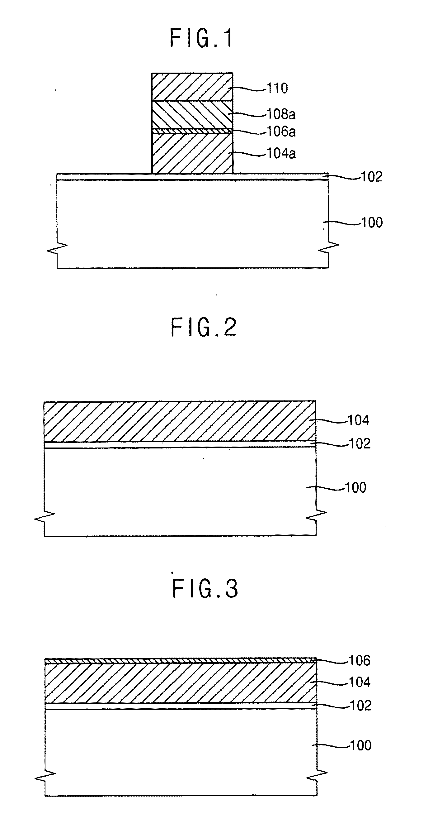
[0037]FIG. 1 is a cross-sectional view illustrating a gate of PMOS transistor in accordance with a first example embodiment.

[0038]Referring to FIG. 1, a substrate 100 that may include a semiconductor material such as silicon is prepared.

[0039]A gate oxide layer 102 may be formed on the substrate 100. In this example embodiment, the gate oxide layer 102 may include silicon oxide formed by thermally oxidizing a surface of the substrate 100. Alternatively, the gate oxide layer 102 may include silicon oxide having a nitridated surface. When the gate oxide layer 102 includes silicon oxide having a nitridated surface, ions or metal may be prevented from diffusing into the substrate 100 through the gate oxide layer 102.

[0040]A first conductive layer pattern 104a may be formed on the gate oxide layer 102. The first conductive layer pattern 104a may include polysilicon doped with boron.

[0041]A diffusion preventing layer pattern 106a may be formed on the first conductive layer pattern 104a to...

example embodiment ii

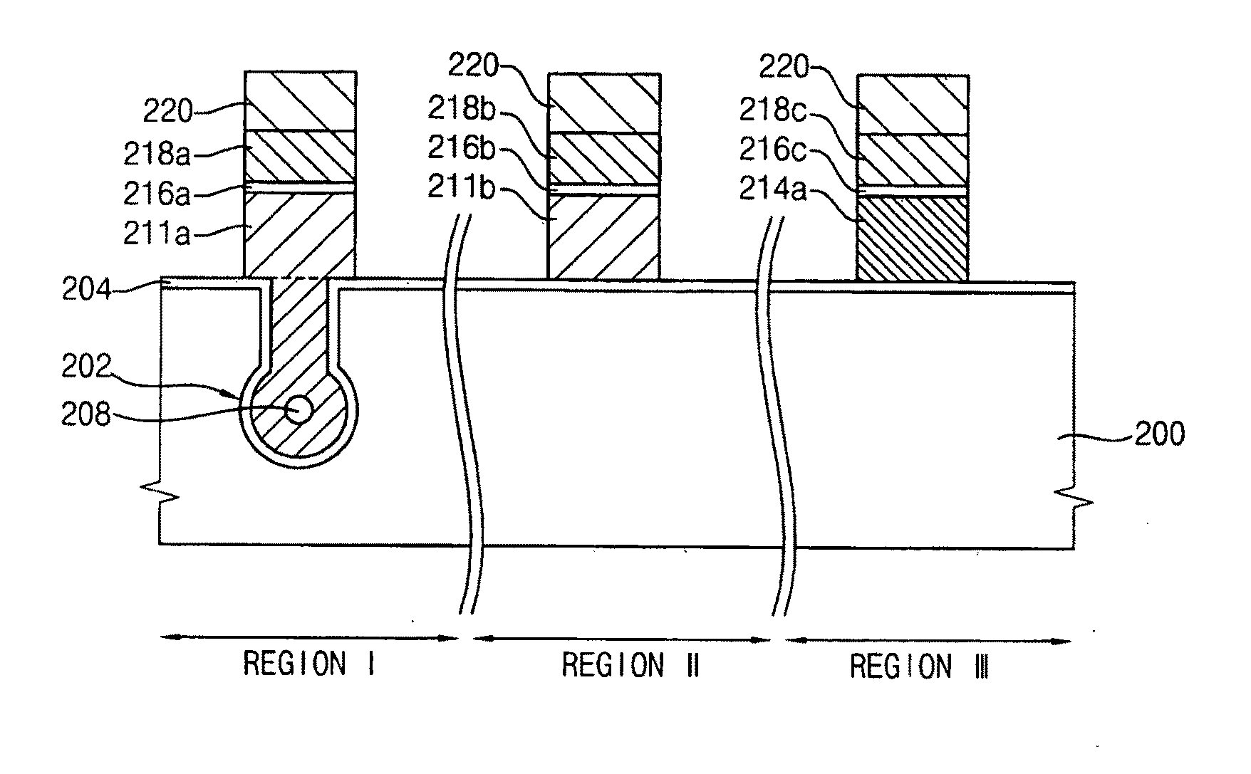
[0063]FIG. 6 is a cross-sectional view illustrating gates of a DRAM device in accordance with a second example embodiment.

[0064]The DRAM device described hereinafter may include at least one n-type transistor on a cell region, and at least an n-type transistor and / or a p-type transistor on a peripheral circuit region. Also, at least one n-type transistor on the cell region may include a recessed gate. The n-type transistor and the p-type transistor on the peripheral circuit region may each include a planar type transistor.

[0065]Referring to FIG. 6, a substrate 200 including a semiconductor material, such as silicon, may be prepared.

[0066]The substrate 200 may be divided into three regions. N-type transistors serving as a unit cell may be formed on a first region. N-type transistors serving as a peripheral circuit for driving the unit cell may be formed on a second region. P-type transistors serving as a peripheral circuit for driving the unit cell may be formed on a third region.

[00...

example 1

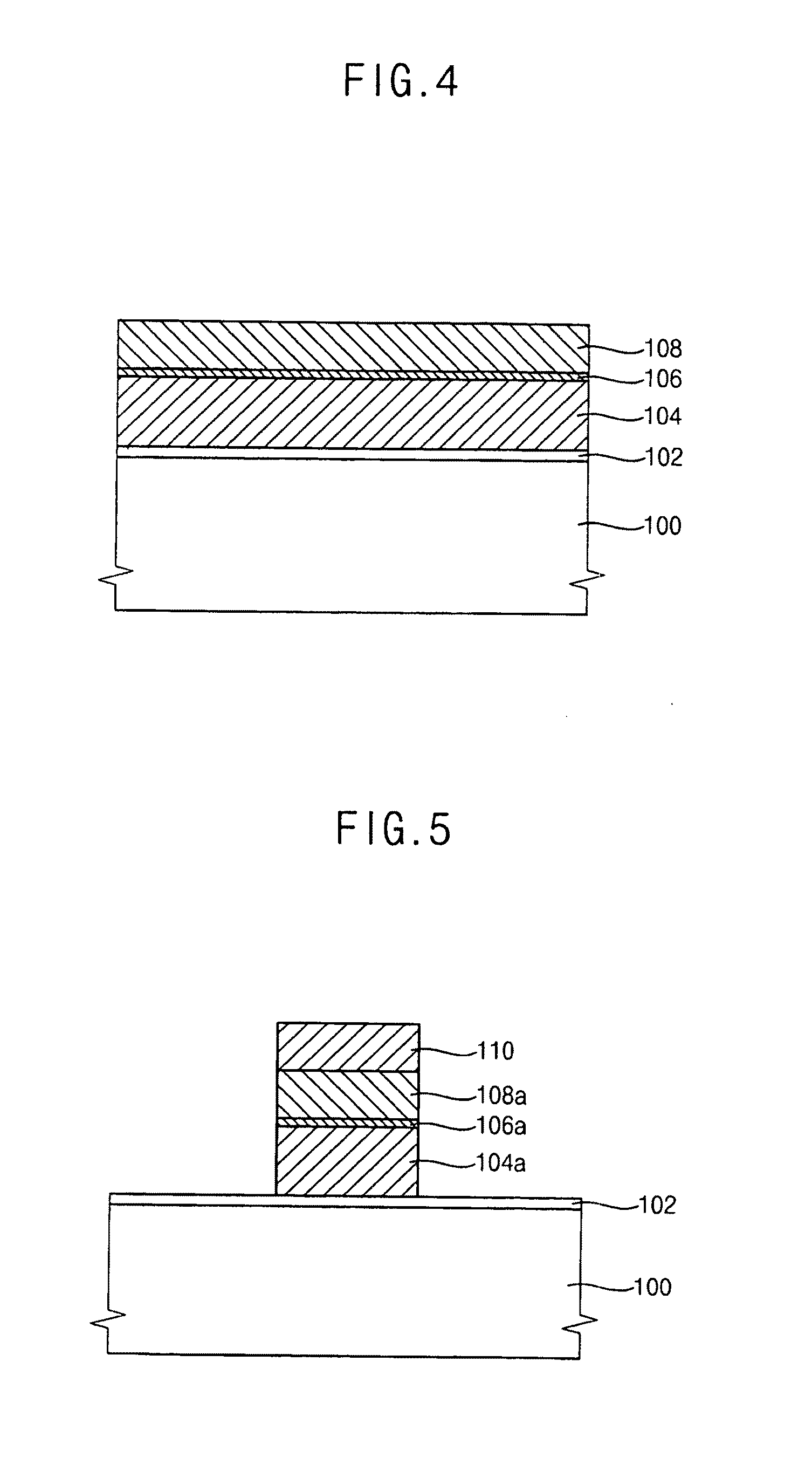
[0112]An amorphous silicon layer was formed on a bulk substrate using a reaction gas including trisilane (Si3H8) by a chemical vapor deposition (CVD) process.


PUM


Abstract

A gate of a transistor includes a gate oxide layer formed on a semiconductor device, a first conductive layer pattern including polysilicon doped with boron and formed on the gate oxide layer, a diffusion preventing layer pattern including amorphous silicon formed by a chemical vapor deposition process using a reaction gas having trisilane (Si3H8) and formed on the first conductive layer pattern, and a second conductive layer pattern including metal silicide and formed on the diffusion preventing layer pattern. Since a gate of PMOS transistor includes a diffusion preventing layer having an excellent surface morphology, diffusion of impurities is sufficiently prevented. Thus, the threshold voltage of PMOS transistor may be reduced and threshold voltage distribution may be improved.

Description

PRIORITY STATEMENT[0001]This application is a divisional of U.S. patent application Ser. No. 11 / 892,223, filed on Aug. 21, 2007, which claims priority under 35 USC §119 to Korean Patent Application No. 10-2006-0079422, filed on Aug. 22, 2006, in the Korean Intellectual Property Office (KIPO), the entire contents of each of which are herein incorporated by reference.BACKGROUND[0002]1. Field[0003]Example embodiments relate to a gate of a transistor and a method of forming the same, for example to a gate of a PMOS transistor and a method of forming the gate.[0004]2. Description of Related Art[0005]In conventional processes for manufacturing a semiconductor device, polysilicon doped with n-type impurities, such as phosphorous, antimony, etc., may be used as a gate electrode for either a positive channel metal oxide semiconductor (PMOS) transistor or a negative channel metal oxide semiconductor (NMOS) transistor.[0006]However, since a buried channel may be formed in a PMOS transistor tha...

Claims


Application Information

Patent Timeline
Patent Type & Authority Applications(United States)
IPC IPC(8): H01L21/28
CPCH01L21/82345H01L21/82385H01L21/823842H01L21/823456H01L21/18
Inventor KIM, JIN-GYUNHWANG, KI-HYUNYANG, SANG-RYOL
Owner KIM JIN GYUN
Learn More