Semiconductor photodiode device and manufacturing method thereof

Inactive Publication Date: 2011-02-10
HITACHI LTD
View PDF4 Cites 48 Cited by
  • Summary
  • Abstract
  • Description
  • Claims
  • Application Information

AI Technical Summary

Benefits of technology

[0005]Optical communication has become predominant in broad band networks of internets that form a part of the foundation of modern information society. In the optical communication system, near infrared (IR) light in a range of 800 nm to 1600 nm is used. A particularly important wavelength band is a band where loss of optical fibers is minimized, and 850 nm is used for short distant communication and 1310 nm and 1550 nm are used for long distance communication. For photodiodes in the optical communication, compound semiconductors, mainly, gallium arsenide (GaAs) and indium phosphide (InP) having good light absorption characteristics in the long wavelength band have been used. However, for further popularization of future optical communication systems, it is essential to reduce the cost and the size and, further, improve the performance of apparatus, and technical innovation is demanded also for the photodiodes in order to attain such demands.
[0006]In view of the background described above, a photodiode using germanium (Ge) is note worthy. Ge belongs to the same IV group semiconductor as silicon (Si) which is an essential material for modern integrated circuits having a matching property with matured silicon processes and, in addition, has a bandgap at a room temperature of 0.6 eV which is smaller than 1.1 eV of that of Si, and can absorb light up to 1600 nm. Accordingly, Ge is a material that can provide a possibility for fusion of optical devices and electronic devices.
[0007]For photodiodes in the optical communication, compatibility is required between the high speed performance conforming to modulation signals at high speed and high efficiency performance of converting more optical signals into electric signals, and research and development have been progressed also for Ge photodiodes with an identical point of view. In the wavelength band of 1550 nm used for long distance communication, an absorption length defined by a distance till the amount of absorbed light is attenuated to 1 / e is about 2 μm in a case of Ge and a sufficient thickness is required for the photoreceiving portion. However, since the high speed performance depends on the inter-electrode distance of the photodiode, the high speed performance is degraded more as the distance between p / n electrodes is increased. Therefore, for attaining the high speed performance and the high efficiency performance together, a technical break through for overcoming the trade-off relation has been required. One of means for solving the subject is disclosed in JP-T No. 2007-527626. FIG. 2 shows the structure of this existent example 1. FIG. 2A is a view showing a cross section of a Ge photodiode in the existent example 1. In an SOI (Silicon On Insulator) substrate in which a silicon dioxide (SiO2) layer 102 and an upper Si layer 103 are formed on an Si substrate 101, Ge layer 104 is formed by epitaxial growing in a region surrounded by an SiO2 film 105, and p-type and n-type ion implantation regions 106 and 107 are alternately formed intermittently in the upper portion of the Ge layer 104. FIG. 2B is a plan view showing a photodiode device structure of the existent example 1 on the side of the substrate surface, and FIG. 2A corresponds to a cross section of FIG. 2B along line a in FIG. 2B. Since the implantation regions can be formed deeply in the Ge layer and the distance between p / n electrodes can also be shortened, the time in which electron-hole pairs generated by light absorption reach the electrodes can be shortened while ensuring a sufficient thickness of the light absorption layer. As described above, a plurality of means have been proposed for improving the trade-off relation and the performance of the Ge photodiodes has been improved every year.

Problems solved by technology

However, since the high speed performance depends on the inter-electrode distance of the photodiode, the high speed performance is degraded more as the distance between p / n electrodes is increased.
Since a problem such as increase of a noise index results in the amplification by the electric circuit in a case of amplifying small signals, it is necessary to amplify optical signals and convert them into electric signals.
However, the avalanche photodiode requires high operation voltage in view of the characteristics that it is used in an electric field region of avalanche amplification, and is poor in view of low power consumption performance.
Further, the amplification performance is in a trade-off relation with the high speed operation performance, and an upper limit value is present for a GB product as a product of an amplifiable frequency and an amplification factor.
Accordingly, in an application use of requiring light amplification, optical signals are once converted into electric signals by a usual photodiode using a compound semiconductor and then the electric signals are amplified by an Si avalanche diode of higher GB product, which results problems such as increase in the number of production steps, increase of the chip size, and lowering of the flexibility upon circuit design.

Method used


Image

  • Semiconductor photodiode device and manufacturing method thereof
  • Semiconductor photodiode device and manufacturing method thereof
  • Semiconductor photodiode device and manufacturing method thereof

Examples


first embodiment

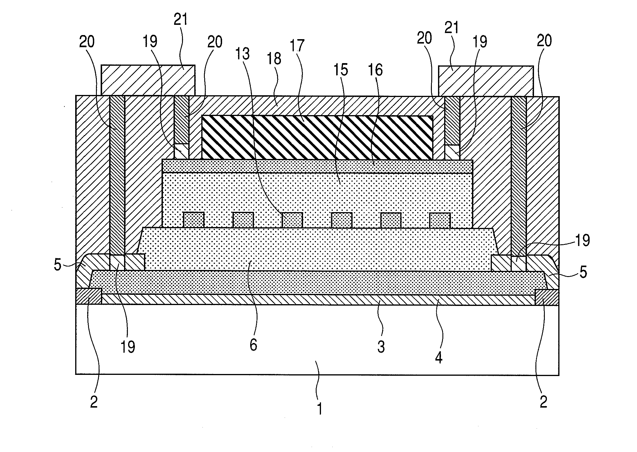
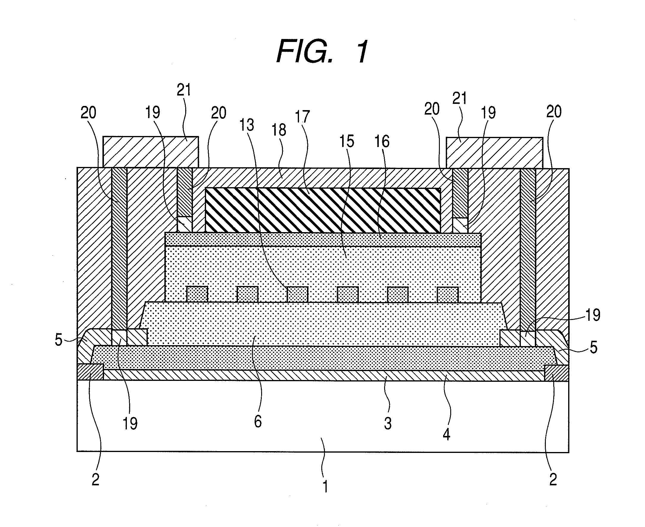
[0104]FIG. 1 is a cross sectional view showing a first embodiment of a semiconductor photodiode device according to the invention. This cross sectional structure shows a cross section of a photoreceiving portion in a bipolar phototransistor having a photoreceiving portion and an amplification portion separately.

[0105]FIG. 1 shows a silicon substrate 1 and an insulating film 2 having a trench. Above the insulation film 2, an n-type Ge layer 4 is formed by way of a buffer layer 3 for improving the crystallinity of upper layers. A high resistance Ge layer 6 is formed within the trench formed with an insulating film 5 above the Ge layer 4, and a p-type Ge layer 13 divided at a predetermine distance in the direction horizontal to the substrate and a high resistance Ge layer 15 are formed in the layer thereabove. An n-type Ge layer 16 is formed above the high resistance Ge layer 15. A silicon nitride film (Si3N4) 17 and an interlayer insulating film 18 are also shown. Metal electrode 19 t...

second embodiment

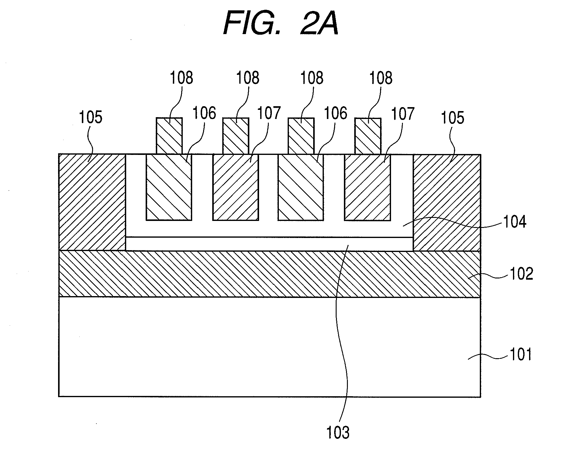
[0117]FIG. 8A to FIG. 8D are views for the cross sectional structure showing a second embodiment of a semiconductor photodiode according device to the invention along a photodiode device manufacturing steps. In FIG. 8A to FIG. 8D, portions having same functions as those in the first embodiment carry identical references with those in the first embodiment. The manufacturing steps are to be described sequentially.

[0118]At first, an insulating film 22 is deposited above an Si substrate 1, and patterning is applied to remove the insulating film 22 by etching while leaving a predetermined region. Further, an insulating film 23 is deposited and a trench is formed to the insulating film 22 to obtain a structure shown in FIG. 8A. It is preferred to use, for example, Si3N4 for the insulating film 22 and use, for example, SiO2 for the insulating film 23. In this case, the Si3N4 film 22 may be fabricated by dry etching using sulfur hexafluoride (SF6) and the SiO2 film 23 may be fabricated by d...

third embodiment

[0123]This embodiment discloses a photodiode device structure in which the capacitance of the bipolar portion in the photodiode device is decreased, and the manufacturing method thereof. FIG. 9A to FIG. 9I are cross sectional views showing the manufacturing process of the semiconductor photodiode device in this embodiment. Drawings show cross sections including the bipolar portion. While only one bipolar portion is shown in FIG. 9A to FIG. 9I for avoiding complexity, the bipolar portion may be present also in the opposite direction of the photoreceiving portion putting the portion therebetween.

[0124]At first, after depositing an insulating film 22 over an Si substrate 1 as shown in FIG. 9A, patterning is applied to leave the insulating film 22 while leaving only for the electrode fainting portions of the collector region in the bipolar portion and the n-type Ge layer in the photoreceiving portion and eliminating the remaining portions by etching. In the same manner as in the second ...


PUM


Abstract

A semiconductor photodiode includes a semiconductor substrate; a first conduction type first semiconductor layer formed above the semiconductor substrate; a high resistance second semiconductor layer formed above the first semiconductor layer; a first conduction type third semiconductor layer formed above the second semiconductor layer; and a second conduction type fourth semiconductor layer buried in the second semiconductor layer, in which the fourth semiconductor layer is separated at a predetermined distance in a direction horizontal to the surface of the semiconductor substrate.

Description

CLAIM OF PRIORITY[0001]The present application claims priority from Japanese patent application JP 2009-184003 filed on Aug. 7, 2009, the content of which is hereby incorporated by reference into this application.FIELD OF THE INVENTION[0002]The present invention relates to a semiconductor photodiode device which is a photodiode device using a germanium containing semiconductor and a manufacturing method thereof, and it particularly relates to a semiconductor photodiode device such as a germanium-phototransistor having a high sensitivity and a high speed performance, as well as a manufacturing method thereof.BACKGROUND OF THE INVENTION[0003]In existent semiconductor photodiode devices, there has been a technique for overcoming a trade-off relation of the thickness and the inter-p / n electrode distance required for the photoreceiving portion thereby attaining both high speed performance and high efficiency performance (for example, refer to JP-T-2007-527626).[0004]Further, in existent ...

Claims


Application Information

Patent Timeline
IPC IPC(8): H01L31/10H01L31/18
CPCH01L21/02381H01L21/0245H01L21/02502H01L21/02532Y02E10/547H01L31/028H01L31/103H01L31/1124H01L31/1808H01L21/02639
Inventor MIURA, MAKOTOSAITO, SHINICHILEE, YOUNGKUNODA, KATSUYA
Owner HITACHI LTD
Why Eureka
Try Eureka