
Superconductive Article with Prefabricated Nanostructure for Improved Flux Pinning

a technology of nanostructure and superconducting article, which is applied in the direction of superconducting magnet/coil, superimposed coating process, magnetic body, etc., can solve the problems of tape significantly affecting the critical current, tape does not represent a widespread commercially feasible product, and continues to exis

Active Publication Date: 2011-02-03
SUPERPOWER INC
View PDF11 Cites 9 Cited by
  • Summary
  • Abstract
  • Description
  • Claims
  • Application Information

AI Technical Summary

Benefits of technology

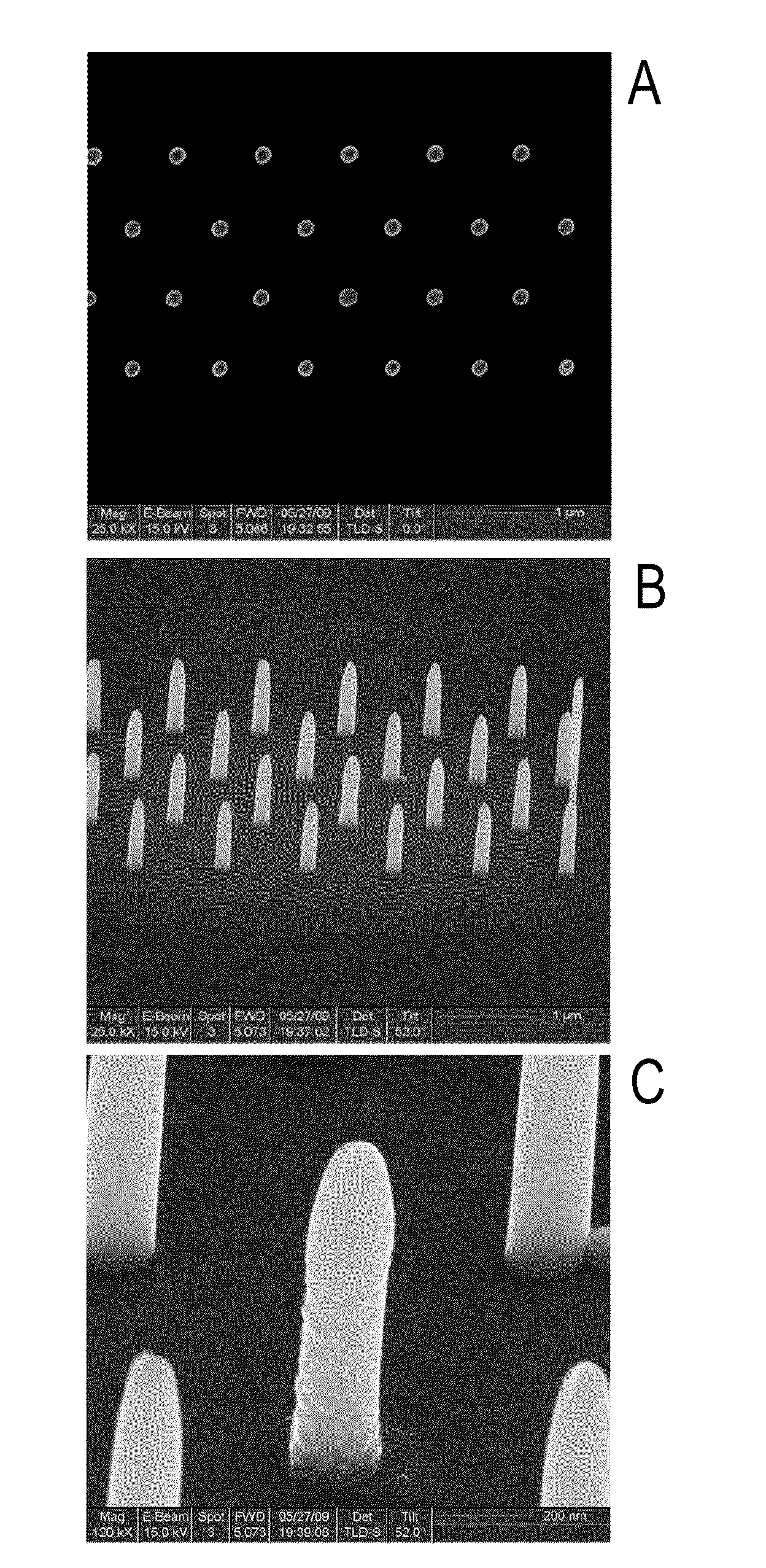
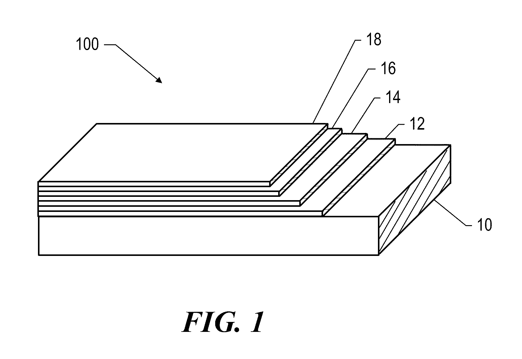
[0009]In an embodiment, a superconducting article includes a substrate; a buffer layer overlying the substrate; and a high-temperature superconducting (HTS) layer overlying the buffer layer. The HTS layer can include a plurality of nanorods. In a embodiment, each of the plurality of nanorods can extend at least about 50% of the thickness of the HTS layer. In another embodiment, the nanorods can be substantially parallel to one another. In yet another embodiment, the plurality of nanorods can form an ordered array.
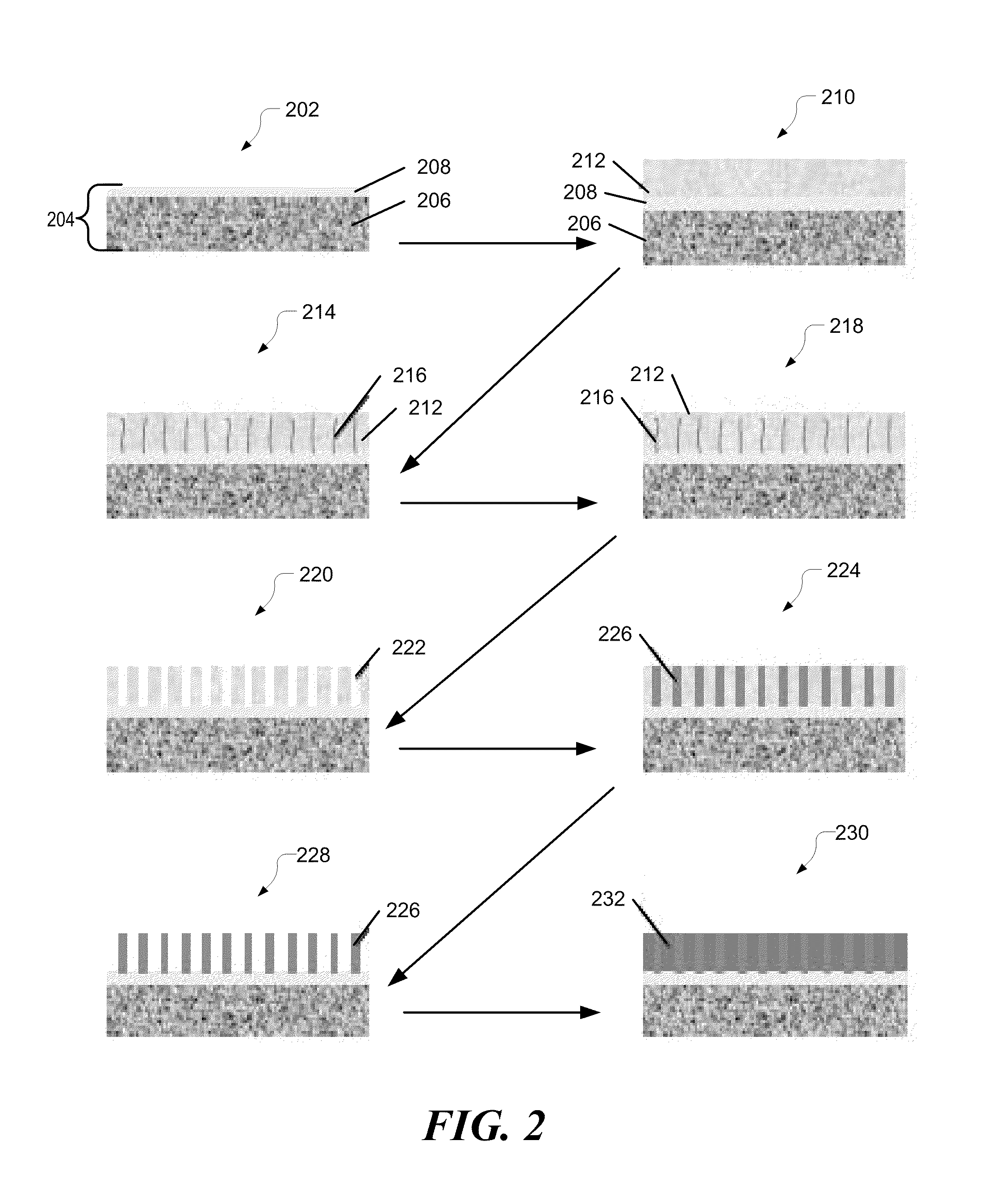
[0010]In another embodiment, a method of forming a superconducting article includes providing a substrate tape, forming a buffer layer overlying the substrate tape, forming a plurality of nanorods, and depositing a high-temperature superconducting (HTS) layer around the plurality of nanorods overlying the buffer layer. In a embodiment, forming the plurality of nanorods can include applying a polymer coating, forming nanoholes through the polymer coating, electrodepositing a metal within the nanoholes to form nanorods, and removing the polymer coating. In another embodiment, forming the plurality of nanorods can include forming a nanoporous layer overlying the buffer layer, electrodepositing a metal into an array of nanopores within the nanoporous layer to form nanorods, and removing the nanoporous layer. In yet another embodiment, forming the plurality of nanorods can include forming a nanodot array overlying the buffer layer and depositing an array of nanorods nucleated by the nanodot array. In a further embodiment, forming the plurality of nanorods can include evaporating nanorod material to form a material cloud, and directing an electron beam through the material cloud towards the substrate tape, thereby depositing an array of nanorods overlying the buffer layer.

Problems solved by technology

However, it was not until somewhat recently that oxide-based high-temperature (high-tc) superconductors have been discovered.
While such potential benefits of high-temperature superconductors remain quite compelling, numerous technical challenges continue to exist in the production and commercialization of high-temperature superconductors on a large scale.
Among the challenges associated with the commercialization of high-temperature superconductors, many exist around the fabrication of a superconducting tape segment that can be utilized for formation of various power components.
Although such conductors may be made in extended lengths needed for implementation into the power industry (such as on the order of a kilometer), due to materials and manufacturing costs, such tapes do not represent a widespread commercially feasible product.
However, to date, numerous engineering and manufacturing challenges remain prior to full commercialization of such second generation-tapes and devices incorporating such tapes.
Further, the angle of the magnetic field to the tape significantly affects the critical current.
One particular challenge is to reduce the effect of magnetic fields on the critical current of the HTS tape.
Therefore, another challenge is to improve the critical current in field orientations other than that parallel to the tape.

Method used


Image

  • Superconductive Article with Prefabricated Nanostructure for Improved Flux Pinning
  • Superconductive Article with Prefabricated Nanostructure for Improved Flux Pinning
  • Superconductive Article with Prefabricated Nanostructure for Improved Flux Pinning

Examples


second embodiment

[0041]In a second embodiment, nanorods can be formed using a nanoporous template. FIG. 4 illustrates an exemplary process of using nanoporous templates to form a prefabricated nanostructure with the HTS layer. At 402, a substrate 404 and a buffer layer 406 are provided. Additionally, an aluminum layer 408 is deposited overtop the buffer layer 406. For example, the aluminum layer can be deposited by sputtering or thermal evaporation. At 410, an anodic oxidation process can convert the aluminum layer 408 into an anodized aluminum oxide layer 412 including a highly ordered array of nanopores 414. At 416, metal, such as nickel or gold, can be electrodeposited within the nanopores 414 forming nanorods 418. At 420, the aluminum oxide layer 412 is removed by etching, leaving the nanorods 418 attached to the buffer layer 406. At 424, HTS material can be deposited to form an HTS layer 426 surrounding the nanorods 418. The HTS material can be deposited using one of the various techniques know...

third embodiment

[0043]In a third embodiment, chemical vapor deposition or chemical solution deposition can be used to form nanorods on predefined nucleation sites. For example, a nanodot array using materials such as colloidal gold particles or similar material can be deposited on the buffer surface as a nucleation site for the nanorods. Vapor-solid-liquid phase growth can be employed to grow the nanorods using the nanodots as a nucleation site. For example, ZnO can be mixed with graphite and vaporized. The vaporized material can be deposited on the nanodot templates. The spacing and density of the nanorods can depend on the spacing and density of the nanodots. The diameter and length of the nanorods can depend on the vaporization temperature and time and the deposition temperature and time. Other materials such as magnetic oxides can be used to form the nanorods that could lead to ferromagnetic pinning. Further, HTS material can be deposited around the nanorods to form an HTS layer embedding the n...


PUM

PropertyMeasurementUnit
diameteraaaaaaaaaa
diameteraaaaaaaaaa
heightaaaaaaaaaa

Abstract

A superconducting article comprises a substrate, a buffer layer overlying the substrate, and a high-temperature superconducting (HTS) layer overlying the buffer layer. The HTS layer includes a plurality of nanorods. A method of forming a superconducting article comprises providing a substrate, depositing a buffer layer overlying the substrate; forming a nanodot array overlying the buffer layer; depositing an array of nanorods nucleated on the nanodot array; and depositing a high-temperature superconducting (HTS) layer around the array of nanorods and overlying the buffer layer.

Description

CROSS-REFERENCE TO RELATED APPLICATIONS[0001]This application claims the benefit under 35 U.S.C. §119(e) of U.S. Provisional Patent Application No. 61 / 229,225 filed Jul. 28, 2009, the disclosure of which is hereby incorporated herein by reference.STATEMENT REGARDING FEDERALLY SPONSORED RESEARCH OR DEVELOPMENT[0002]Not applicable.FIELD OF THE INVENTION[0003]The present disclosure generally relates to superconducting articles, and more specifically relates to a superconducting article with prefabricated nanostructure for improved flux pinning.BACKGROUND OF THE INVENTION[0004]Superconductor materials have long been known and understood by the technical community. Low-temperature superconductors (low-tc or lts) exhibiting superconducting properties at temperatures requiring use of liquid helium (4.2 k), have been known since 1911. However, it was not until somewhat recently that oxide-based high-temperature (high-tc) superconductors have been discovered. Around 1986, a first high-temper...

Claims


Application Information

Patent Timeline
Patent Type & Authority Applications(United States)
IPC IPC(8): H01L39/02H01L39/24H10N60/80H10N60/01H10N60/20H10N60/85
CPCH01L39/143H01L39/2461H01L39/2483B82Y40/00Y10T428/26C23C28/322C23C28/345Y10T428/25B82Y30/00H10N60/203H10N60/0632H10N60/0828Y02E40/60B82B3/00H10N60/80H10N60/85
Inventor SELVAMANICKAM, VENKATMAJKIC, GORANMARTCHEVSKII, MAXIM
Owner SUPERPOWER INC
Learn More