Method of fabricating oxide thin film transistor

Active Publication Date: 2010-12-02
LG DISPLAY CO LTD
View PDF8 Cites 50 Cited by
  • Summary
  • Abstract
  • Description
  • Claims
  • Application Information

AI Technical Summary

Benefits of technology

[0027]Another object of the present invention is to provide a method of fabricating an oxide thin-film transistor in which a channel protection layer is formed using a simple process without deteriorating the oxide semiconductor by depositing an insulation layer having an oxide characteristic in-situ through controlling oxygen (O2) flow subsequent to depositing an oxide semiconductor.
[0030]As described above, according to a method of fabricating an oxide thin-film transistor in accordance with the present invention, an amorphous zinc oxide-based semiconductor is used as an active layer to provide excellent uniformity, thereby providing an effect that can be applied to large-sized displays.
[0031]At this time, the foregoing amorphous zinc oxide-based semiconductor may be damaged on a back channel region thereof while performing subsequent processes, but according to a method of fabricating an oxide thin-film transistor in accordance with the present invention, a channel protection layer is formed using a simple process without deteriorating the oxide semiconductor by collectively depositing an insulation layer having an oxide characteristic in-situ within a sputter through controlling oxygen flow subsequent to depositing the oxide semiconductor. As a result, it can provide an effect that the fabrication process and cost thereof are reduced by decreasing the tact time and the number of masks as well as provide an effect of enhancing the element characteristics.

Problems solved by technology

However, the foregoing liquid crystal display device has been the most-spotlighted display element due to light-weight and low power consumption, the liquid crystal display device is not a light-emitting element but a light-receiving element and have technical restrictions in brightness, contrast ratio, viewing angle, and the like, and as a result, the development of new display elements for overcoming such disadvantages have been actively carried out.
An amorphous silicon thin-film transistor used in the foregoing liquid crystal display device can be fabricated with low-temperature processes but has very low mobility and does not satisfy a constant current bias condition.
On the contrary, a multi-crystalline silicon thin-film transistor has high mobility and a satisfactory constant current bias condition whereas it is difficult to make large-sized displays and also required to have high-temperature processes because it is difficult to attain a uniform characteristic.
Due to this, an oxide semiconductor thin-film transistor in which an active layer is formed with an oxide semiconductor has been developed, but it has a problem that the oxide semiconductor thin-film transistor may be damaged and transformed during an etching process of the source / drain electrodes thereof in case of applying the oxide semiconductor to a thin-film transistor having an existing bottom gate structure.
As described above, an oxide semiconductor has a weak coupling structure and thus an etch stopper 50 is additionally formed as a barrier layer over the active layer 24 to prevent the back channel region from being damaged by subsequent processes after depositing the oxide semiconductor, but it has a disadvantage of complicating the process as well as increasing the cost.
At this time, since the patterning of the active layer 24 and the deposition of the insulation layer are progressed in a state that the vacuum of the vacuum chamber is released, the oxide semiconductor may be exposed to the air as well as brought into contact with chemical materials while being subject to the photo process, thereby causing the back channel region to be damaged.
As a result, the element characteristics are deteriorated, and also a tact time is increased by the movement between chamber devices while depositing the insulation layer.

Method used


Image

  • Method of fabricating oxide thin film transistor
  • Method of fabricating oxide thin film transistor
  • Method of fabricating oxide thin film transistor

Examples


first embodiment

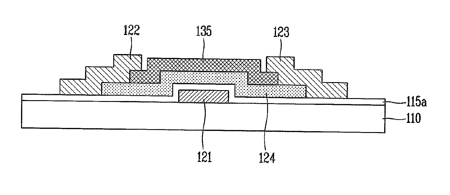
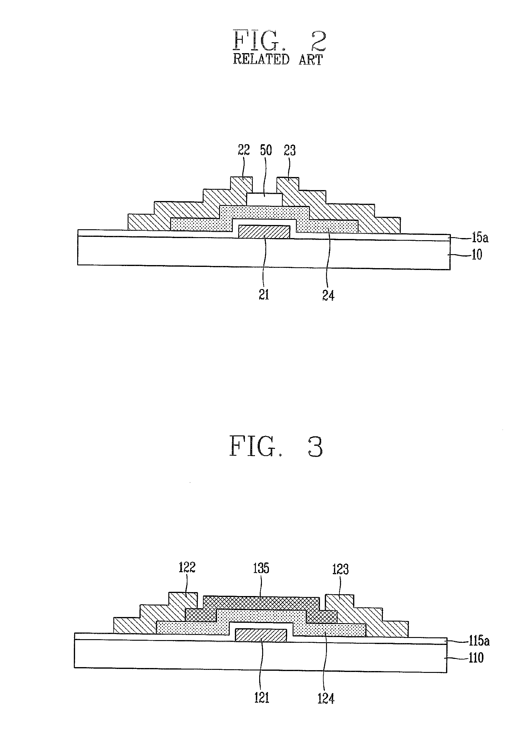
[0061]FIGS. 5A through 5E are cross-sectional views specifically illustrating a second mask process according to the present invention.

[0062]As illustrated in FIG. 5A, a insulation layer 115a, which is made of an inorganic insulation film such as a silicon nitride (SiNx) film, a silicon oxide (SiO2) film and the like, or an high-dielectric oxide film such as a hafnium (Hf) oxide, aluminum oxide and the like, is formed on an entire surface of the substrate 110 formed with the gate electrode 121.

[0063]At this time, the insulation layer 115a may be formed by a CVD method using a plasma enhanced chemical vapour deposition (PECVD) system or formed by a physical vapour deposition (PVD) method using a sputtering system.

[0064]Subsequently, a predetermined amorphous zinc oxide-based semiconductor layer 120 is formed by depositing an amorphous zinc oxide-based semiconductor on an entire surface of the substrate 110 formed with the insulation layer 115a using a sputtering system. Then, a prede...

second embodiment

[0079]On the other hand, the active layer and channel protection layer may be formed by using a diffraction mask, and it will be described in detail through the present invention as described below.

[0080]FIGS. 6A through 6F are cross-sectional views specifically illustrating a second mask process according to a second embodiment of the present invention.

[0081]As illustrated in FIG. 6A, a insulation layer 215a, which is made of an inorganic insulation film such as a silicon nitride film, a silicon oxide film and the like, or an high-dielectric oxide film such as a hafnium oxide, aluminum oxide and the like, is formed on an entire surface of the substrate 210 formed with the gate electrode 221.

[0082]Subsequently, a predetermined amorphous zinc oxide-based semiconductor layer 220 is formed by depositing an amorphous zinc oxide-based semiconductor on an entire surface of the substrate 210 formed with the insulation layer 215a using a sputtering system. Then, a predetermined amorphous zi...


PUM


Abstract

According to a method of fabricating an oxide thin-film transistor, when a thin-film transistor is fabricated by using an amorphous zinc oxide (ZnO)-based semiconductor as an active layer, it may be possible to reduce a tact time as well as attain an enhanced element characteristic by depositing an insulation layer having an oxide characteristic in-situ through controlling oxygen (O2) flow subsequent to depositing an oxide semiconductor using a sputter, and the method may include the steps of forming a gate electrode on a substrate; forming a gate insulation layer on the substrate; depositing an amorphous zinc oxide-based semiconductor layer made of an amorphous zinc oxide-based semiconductor and an amorphous zinc oxide-based insulation layer having an oxide characteristic in-situ on the gate insulation layer; forming an active layer made of the amorphous zinc oxide-based semiconductor over the gate electrode while at the same time forming a channel protection layer made of the amorphous zinc oxide-based insulation layer on a channel region of the active layer; and forming a source electrode and a drain electrode electrically connected to a source region and a drain region of the active layer over the active layer.

Description

CROSS-REFERENCE TO RELATED APPLICATIONS[0001]Pursuant to 35 U.S.C. §119(a), this application claims the benefit of earlier filing date and right of priority to Korean Application No. 10-2009-0048770 filed on Jun. 2, 2009, the contents of which is incorporated by reference herein in its entirety.BACKGROUND OF THE INVENTION[0002]1. Field of the Invention[0003]The present invention relates to a method of fabricating an oxide thin-film transistor, and more particularly, to a method of fabricating an oxide thin-film transistor using an amorphous zinc oxide-based semiconductor as an active layer.[0004]2. Description of the Related Art[0005]In recent years, with rising interests in information displays and increasing demands to use portable information media, researches and commercialization of light-weight and thin-profile flat panel displays (FPDs) for substituting traditional displays such as cathode ray tubes (CRTs) have been actively carried out. In particular, among such FPDs, a liqu...

Claims


Application Information

Patent Timeline
IPC IPC(8): H01L21/34
CPCH01L21/02554H01L21/02565H01L21/02592H01L21/02631H01L27/1225H01L29/7869H01L27/1288H01L27/1214H01L29/78606
Inventor KIM, DAE-WONBAE, JONG-UK
Owner LG DISPLAY CO LTD
Why Eureka
Try Eureka