
Shower Plate, Method for Manufacturing the Shower Plate, Plasma Processing Apparatus using the Shower Plate, Plasma Processing Method and Electronic Device Manufacturing Method

a technology for shower plates and plasma processing equipment, which is applied in the field of shower plate manufacturing methods, plasma processing methods and electronic device manufacturing methods, can solve the problems of difficult to perform a uniform process over the whole surface of the substrate to be processed with a high processing rate, uneven plasma formation by a conventional plasma processing apparatus, and limited area with high electron density, etc., to achieve uniform and efficient plasma excitation and microwave degradation

Inactive Publication Date: 2010-09-16
TOKYO ELECTRON LTD +1
View PDF37 Cites 36 Cited by
  • Summary
  • Abstract
  • Description
  • Claims
  • Application Information

AI Technical Summary

Benefits of technology

The present invention provides a shower plate that prevents the back-flow of plasma and ignition phenomena of gas for plasma excitation in a plasma processing apparatus. This is achieved by attaching a ceramic member with a porous-gas passing body to a longitudinal hole used for gas discharge, and setting a pore diameter of the narrow path in the gas flowing path not greater than 10 μm. The shower plate also prevents electric discharge and ignition phenomena caused by microwave in the corner of the gas introduction side of the longitudinal hole. By using a sintered porous-ceramic body with high purity and fine crystal organization, surface flatness can be improved and the problem of electric power efficiency deterioration of plasma excitation caused by the increase of re-combining of an electron and ion of plasma can be solved.

Problems solved by technology

However, plasma formation by a conventional plasma processing apparatus is uneven, and an area with high electron density is limited.
Therefore, there is a problem of difficulty in performing a uniform process over the whole surface of the substrate to be processed with a high processing rate, namely, a throughput.
This problem becomes particularly serious in cases when a substrate having a large diameter is processed.
And in the conventional plasma processing apparatus, since electron temperature is high, a semiconductor device formed on a substrate to be processed was damaged.
The conventional plasma processing apparatus also has some essential problems such as metal contamination by sputtering of a processing chamber wall is large.
Therefore, the conventional plasma processing apparatus is becoming difficult to satisfy a severe requirement against the further refinement of a semiconductor device or a liquid crystal display device and improvement in further productivity.
When plasma flows backwards into the longitudinal hole, there is a problem that abnormal electric discharge and deposition of gas will occur and degradation of transmission efficiency of microwave for exciting plasma and a decline of yield will occur.
However, just making the aperture of the gas discharge hole small is not sufficient enough as a method to prevent the back-flow of plasma.
It is also difficult to form a gas discharge hole of a fine aperture in the shower plate body by hole processing, and there is also a problem of processability.
Therefore, re-combining of an electron and ion of plasma increases, and there is a problem that electric power efficiency of plasma excitation is bad.
However, in this structure, since a general sintered porous-ceramic body sintered at normal temperature and normal pressure is used, the above-mentioned problem generated from badness of surface flatness is not solved.

Method used


Image

  • Shower Plate, Method for Manufacturing the Shower Plate, Plasma Processing Apparatus using the Shower Plate, Plasma Processing Method and Electronic Device Manufacturing Method
  • Shower Plate, Method for Manufacturing the Shower Plate, Plasma Processing Apparatus using the Shower Plate, Plasma Processing Method and Electronic Device Manufacturing Method
  • Shower Plate, Method for Manufacturing the Shower Plate, Plasma Processing Apparatus using the Shower Plate, Plasma Processing Method and Electronic Device Manufacturing Method

Examples


first embodiment

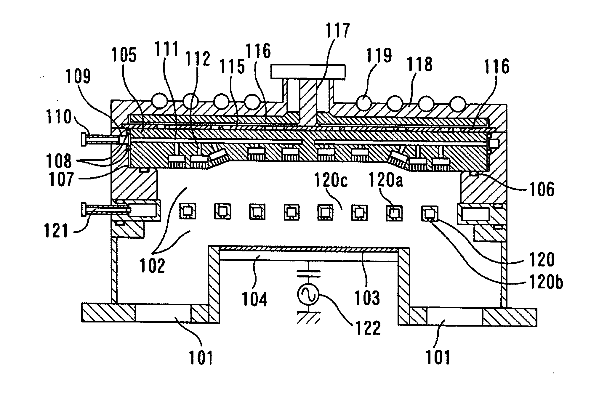
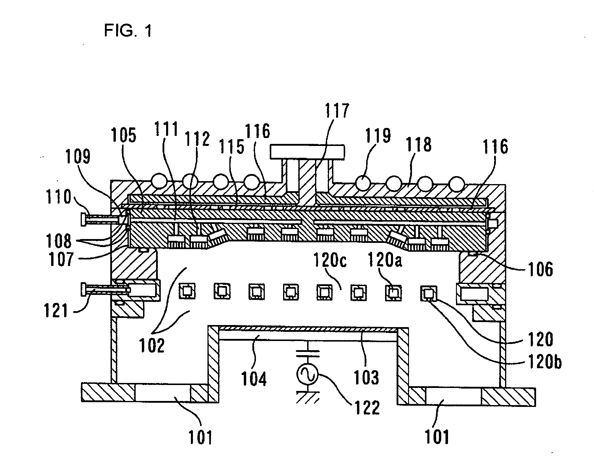
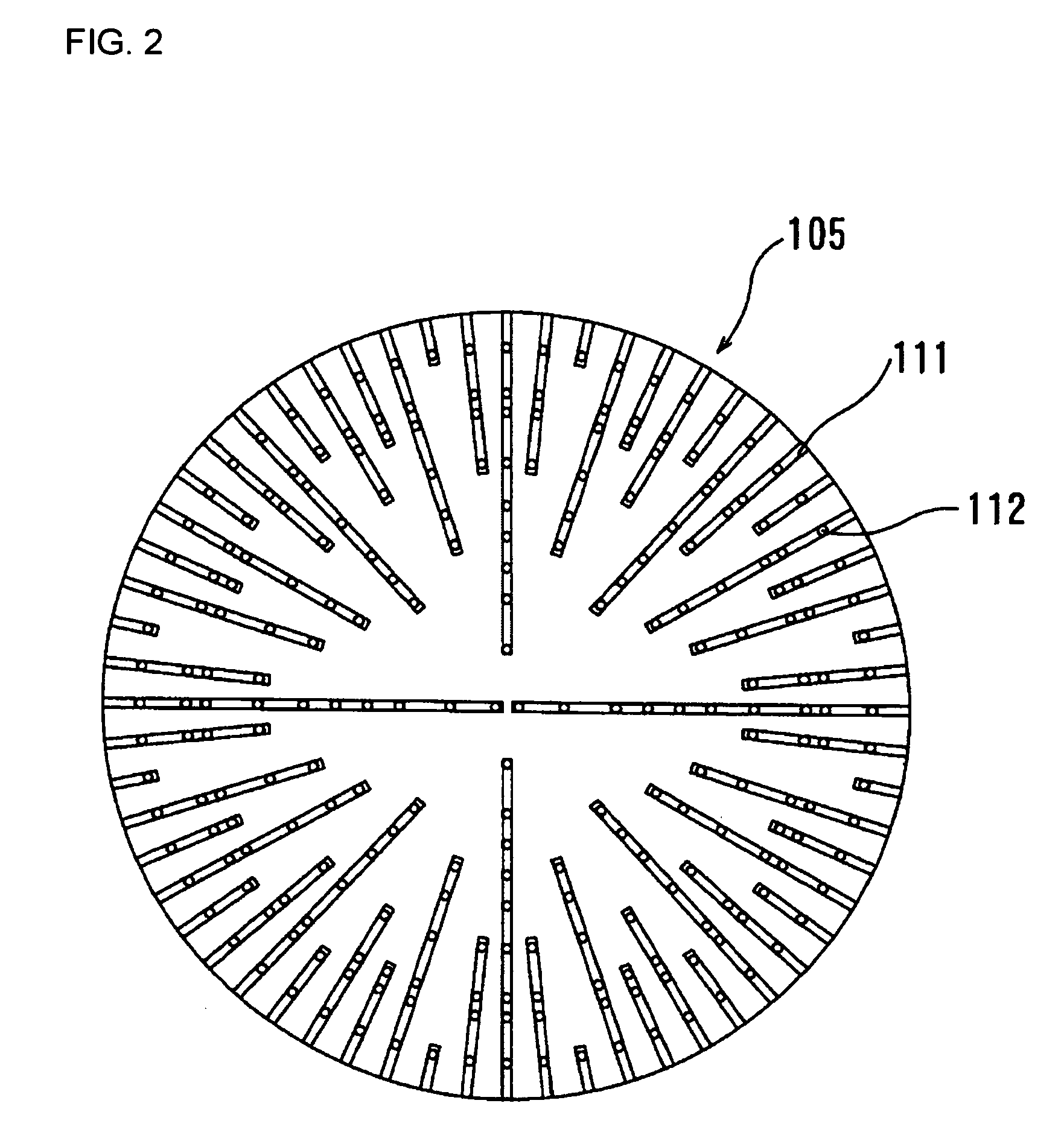
[0037]FIG. 1 illustrates a first embodiment of the present invention. A microwave plasma processing apparatus is illustrated in FIG. 1. An illustrated microwave plasma processing apparatus has a processing chamber 102 in which gas is exhausted via a plurality of exhaust ports 101. In the processing chamber 102, a holding member 104 for holding a substrate to be processed 103 is arranged. In order to uniformly exhaust gas of the processing chamber 102, the processing chamber 102 defines a ring shaped space to the circumference of the holding member 104. The plurality of exhaust ports 101 is arranged in regular intervals to communicate with space, namely, they are arranged in axial symmetry against the substrate to be processed 103. By an arrangement of these exhaust ports 101, gas in the processing chamber 102 can be exhausted more uniformly through the exhaust ports 101.

[0038]A shower plate 105 is fixed onto the upper section of the processing chamber 102 via O-ring for seals 106 at...

second embodiment

[0060]A second embodiment of the present invention is shown in FIG. 5. Referring to FIG. 5, a microwave plasma processing apparatus is shown. The same symbols are attached to the portions, which overlap with the first embodiment, and the explanation will be omitted.

[0061]In this example, in the upper portion of the processing chamber 102, a plate-shaped shower plate 201 is attached via O-ring for seals 106 as a part of outer wall of processing chamber 102 in the position corresponding to the substrate to be processed 103 on the holding member 104. A large number of openings (230 pieces), namely, longitudinal holes 200, have been formed on the plate-shaped shower plate 201. The plate-shaped shower plate 201 is structured by the alumina having a relative permittivity of 9.8 and low microwave dielectric loss (dielectric loss is 1×10⁻⁴ or lower). Further, in the processing chamber 102, a cover plate 202, which is formed of alumina, is attached onto the upper surface side of the shower p...

third embodiment

[0070]A third embodiment of the present invention is shown in FIG. 10. A microwave plasma processing apparatus is shown in FIG. 10. The same symbols are attached to the portions, which overlap with the first and the second embodiments, and the explanation will be omitted. A longitudinal hole 300 of a shower plate 301 in this example is having structure as shown in FIG. 11. That is, a gas discharge hole 300a, 0.05 mm in diameter and 0.5 mm in length, has been opened in the processing chamber 102 side where plasma is excited. The gas introduction side of the gas discharge hole 300a is connected to a hole 300b having diameter of 1 mm. In order to avoid electric field concentration of microwave, a chamfering processing 303 is given to the corner of gas introduction side of the hole 300b. And a sintered porous-ceramic body 302 having a cylindrical shape of height of 5 mm and having a pore that communicates in the gas flow direction is fixed onto the bottom section of the hole 300b having...


PUM

PropertyMeasurementUnit
pore diameteraaaaaaaaaa
diameteraaaaaaaaaa

Abstract

Occurrence of a back-flow of plasma or ignition of gas for plasma excitation in a longitudinal hole portion can be prevented more completely, and a shower plate in which efficient plasma excitation is possible is provided. In shower plate 105, which is arranged in processing chamber 102 of a plasma processing apparatus and discharges gas for plasma excitation into processing chamber, porous-gas passing body 114 having a pore that communicates in the gas flow direction is fixed onto longitudinal hole 112 used as a discharging path of gas for plasma excitation. The pore diameter of a narrow path in a gas flowing path formed of a pore, which communicates to porous-gas passing body 114, is 10 μm or lower.

Description

[0001]This application claims priority under 35 U.S.C. §371 as a National Stage application of PCT application Serial No. PCT / JP2007 / 61857, filed Jun. 13, 2007, entitled “Shower Plate, Method for Manufacturing the Shower Plate, Plasma Processing Apparatus using the Shower Plate, Plasma Processing Method and Electronic Device Manufacturing Method”, which claims priority to Japanese Patent Applications No. P 2006-163357 filed on Jun. 13, 2006, No. P 2006-198754 filed on Jul. 20, 2006 and No. P2007-153563 filed on Jun. 11, 2007, which are incorporated herein by reference.TECHNICAL FIELD[0002]A present invention relates to a plasma processing apparatus. The present invention particularly relates to a shower plate, which is used for a microwave plasma processing apparatus, a manufacturing method of the shower plate, a plasma processing apparatus using the shower plate and a plasma processing method and a manufacturing method of an electronic device.BACKGROUND ART[0003]A plasma treatment ...

Claims


Application Information

Patent Timeline
Patent Type & Authority Applications(United States)
IPC IPC(8): C23F1/08C23C16/00C23F1/00C23C16/455C23C16/511B22F3/12B28B1/00
CPCC23C16/45565C23C16/45568B05B1/18H01J37/3244H01J37/32449C23C16/511
Inventor OKESAKU, MASAHIROGOTO, TETSUYAOHMIISHIBASHI, KIYOTAKA
Owner TOKYO ELECTRON LTD
Learn More