Nano-Scale Biosensors

a biosensor and nano-scale technology, applied in diagnostic recording/measuring, laboratory glassware, instruments, etc., can solve the problems of changing the melting temperature, changing the thermodynamic properties, and requiring expensive fluorescent microscopes to visualize data, etc., to achieve low power, easy to use, and easy to recycle

Inactive Publication Date: 2010-08-12
BOARD OF RGT THE UNIV OF TEXAS SYST
View PDF7 Cites 22 Cited by
  • Summary
  • Abstract
  • Description
  • Claims
  • Application Information

AI Technical Summary

Benefits of technology

[0009]The invention provides a nanotechnology-based low-power, rapid, inexpensive, recyclable, and sensitive electrical detection device, system, and method of sub-femtomolar concentrations of nucleic acids, including genes, with no external sample preparation or labeling or other chemical modification of the sample. The biosensors of the invention may be used in wide variety of applications requiring sensitive nucleic acid detection, including, but not limited to, forensics, early disease detection, disease progression monitoring (such as in response to therapy and / or medicinal agents), legal matters (such as paternity and criminal proceedings), defensive biohazard detection, and immigration issues (such as establishing blood relationships). The biosensors of the invention are useful in further enabling “personalized medicine,” where drugs are designed according to each individual's genetic make-up.

Problems solved by technology

However, these modifications can change the thermodynamic properties of the molecular interactions of DNA and, in some cases, unnaturally stabilize or destabilize the DNA double-strand and change the melting temperature significantly.
Additionally, expensive fluorescent microscopes are needed to visualize the data and normalization of the data to references remain problematic.
Further, the hybridization of the probe and target molecules is a diffusion-limited process requiring long-incubation times as the target molecules must travel to the arrayed probes on the surface of the chip.
While many of the silicon-based sensors can be fabricated with compact size, none of these efforts have resulted in a portable sensor with adequate performance.
The challenges range from the costly and lengthy fabrication processes to the need for external expensive measurement equipment.
The DNA hybridization detection techniques have been implemented on chips but throughput, cost, and multiplexing have not been adequately addressed.
The solid-state DNA interaction detection techniques have also required tagging of target with electrical markers, resulting in possibly altered interactions while requiring sample preparation.

Method used


Image

  • Nano-Scale Biosensors
  • Nano-Scale Biosensors
  • Nano-Scale Biosensors

Examples


example 1

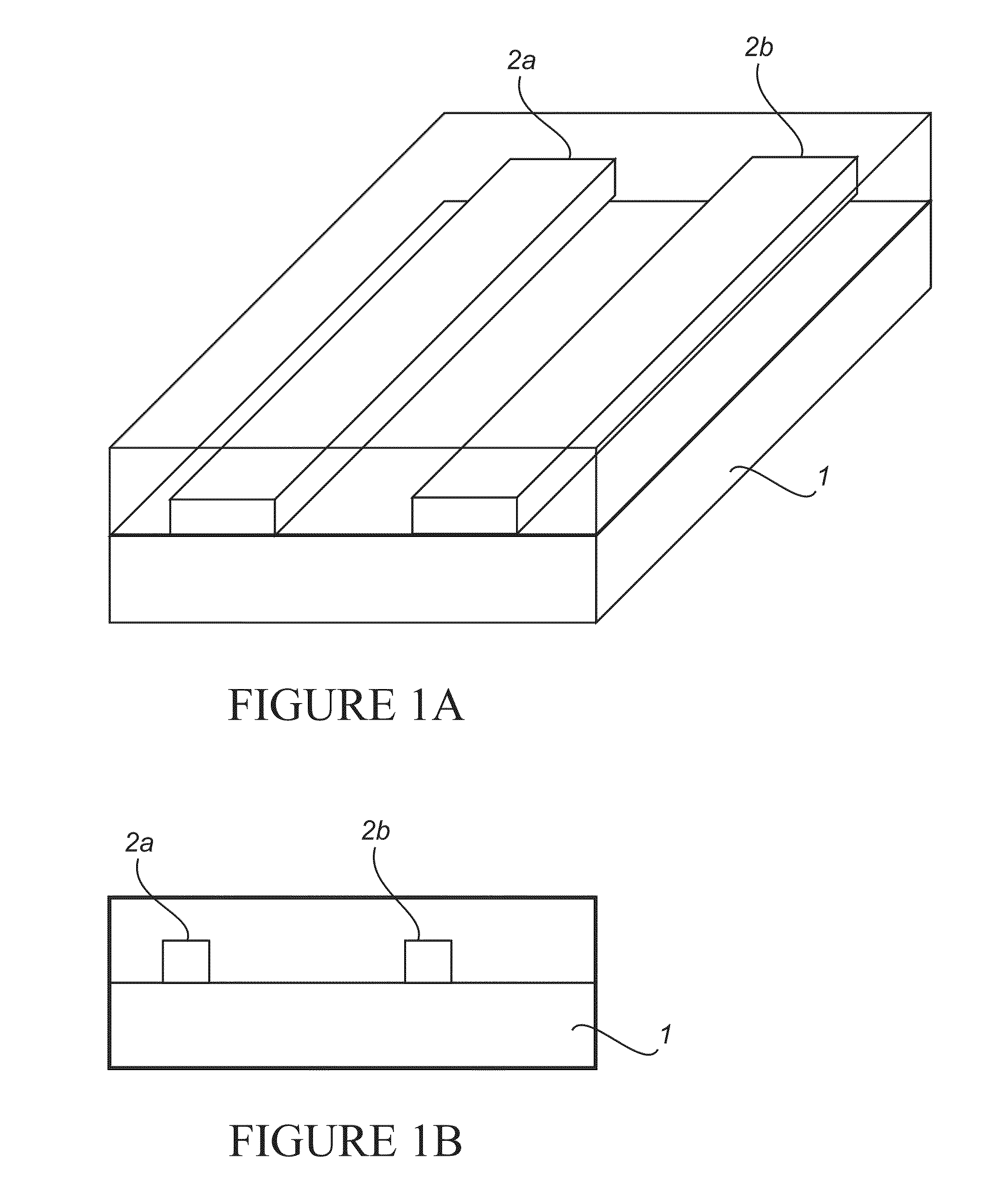
[0446]A two-step photolithography process was used to achieve the structures on a thermally oxidized silicon wafer. In the first step of photolithography, a 3 μm wide line pattern was defined and e-beam evaporation of 50 Å of titanium (as sticky layer) and 150 Å of gold was done (FIG. 15). Lift-off created the metal lines on the wafer. The second optical lithography was done to pattern probing pads aligned to the metal lines. The probing pads were made of 100 Å titanium and 500 Å gold.

[0447]In this example, a manual focused-ion beam (FIB) milling process was performed on metal lines to make a scratch on the surface of the metal. A 30 KV acceleration voltage was used for the FIB scratching using gallium ions. A number of characterization runs were carried out to ensure that FIB does not remove all of the metal line during scratching.

[0448]The FIB based partial scratching of the metal lines creates controlled nano-gaps for break junction fabrication. This ensures a minimal footprint F...

example 2

[0457]The chips with nanoelectrodes were fabricated in two steps of lithography. On the first layer Ti / Au thickness 50 / 150 Å metal pads 500 nm apart were made using e-beam lithography and lift-off. In the second step, optical lithography was done to fabricate probing pads to contact the nanoelectrodes. Bare silicon chips were used to test the attachment and detection schemes prior to using nanoelectrode chips.

[0458]The chips were cleaned in oxygen plasma at 200 W in Ar+O2 and Piranha solution, followed by surface attachment of probe DNA in a nitrogen glovebox with controlled ambience and temperature, as described in S. M. Iqbal, D. Akin, and R. Bashir, Nat. Nanotechnol., 2, 243-8 (2007), incorporated herein by reference. The surface-attached probe molecules were heat cycled in TrisEDTA (TE) buffer three times to ensure all molecules formed hairpin loop structures. The gold nanoparticle reporter conjugates were prepared using thiol-gold chemistry, as described in J. J. Storhoff, R. E...

example 3

Materials

[0485]Chemicals used in this example were purchased from Sigma-Aldrich (St. Louis, Mo.), except that the 3-amino modified DNA strands were purchased from Alpha DNA (Montreal, Quebec). The DNA binding domain from the Bombyx mori retrotransposon protein R2Bm was made in accordance with S. M. Christensen, A. Bibilio, and T. H. Eickbush, Nucl. Acids Res. 33:6461-6468 (2005). The zinc finger and myb motif of the R2Bm protein binds to a specific double stranded DNA sequence (5′-CTTAAGGTAGCAAATGCCTCGTC-3′; SEQ ID NO:4) with the gene coding for the large ribosomal subunit.

Method

[0486]Fabrication of the CMOS Chip: Chips were fabricated in two steps of lithography. On the first layers Ti / Au (thickness 50 Å / 150 Å) metal pads 500 nm apart were made using e-beam lithography. Metal lift-off resulted in well-defined structures. In the second step, optical lithography was used to fabricate probing pads to contact the thin film electrodes.

[0487]Surface modification and attachment of double-...


PUM

PropertyMeasurementUnit
widthaaaaaaaaaa
sizeaaaaaaaaaa
sizeaaaaaaaaaa

Abstract

Devices, systems, and methods for detecting nucleic acid hybridization, including single nucleic base mutations at low concentrations, are disclosed, using surface-tethered hairpin loop oligonucleotide probes and metal-nanoparticles conjugated to a hybridization detection sequence that is capable of binding the stem region of the opened hairpin loop oligonucleotide probe, without the use of labeling or target modification and capable of recycling.

Description

CROSS REFERENCE TO RELATED APPLICATIONS[0001]This application claims the benefit of U.S. Application No. 61 / 150,976, filed Feb. 9, 2009, the disclosure of which is incorporated herein by reference in its entirety.REFERENCE TO GOVERNMENT GRANTS[0002]Portions of the disclosure herein may have been supported, in part, by a grant from the National Science Foundation (CAREER Grant No. ECCS 0845669). The United States Government may have certain rights in this application.FIELD OF THE INVENTION[0003]The invention relates generally to devices, systems, and methods for detecting nucleic acid hybridization, including single nucleic base mutations, are disclosed, using surface-tethered hairpin loop oligonucleotide probes and metal-nanoparticles conjugated to a hybridization detection sequence that is capable of binding the stem of region of the opened hairpin loop oligonucleotide probe, without the use of labeling or target modification.BACKGROUND OF THE INVENTION[0004]Individual genetic muta...

Claims


Application Information

Patent Timeline
Patent Type & Authority Applications(United States)
IPC IPC(8): G01N27/04C23F1/00G03F7/20G01N27/22
CPCA61B5/05C12Q2600/156A61B2562/0285B01L3/502715B01L2300/0636B01L2300/0645B01L2300/0877B01L2300/1827B82Y15/00B82Y30/00C12Q1/6825G01N27/021A61B5/14546C12Q2600/106C12Q1/6886C12Q2565/629C12Q2563/155C12Q2525/301
Inventor IQBAL, SAMIR M.GOYAL, SWATICHRISTENSEN, SHAWN M.NOOR, MOHAMMUD R.
Owner BOARD OF RGT THE UNIV OF TEXAS SYST
Why Eureka
Try Eureka