
Chemically sensitive field effect transistors and uses thereof in electronic nose devices

a field effect transistor and chemically sensitive technology, applied in the field of electronic nose devices, can solve the problems of difficulty in real-time measurement of minute quantities of vocs, degree of expertise required, and need for expensive equipmen

Active Publication Date: 2010-08-05
TECHNION RES & DEV FOUND LTD
View PDF47 Cites 93 Cited by
  • Summary
  • Abstract
  • Description
  • Claims
  • Application Information

AI Technical Summary

Benefits of technology

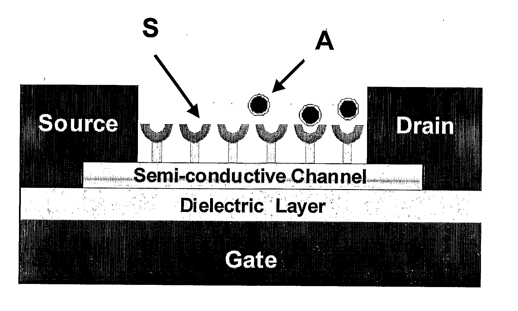
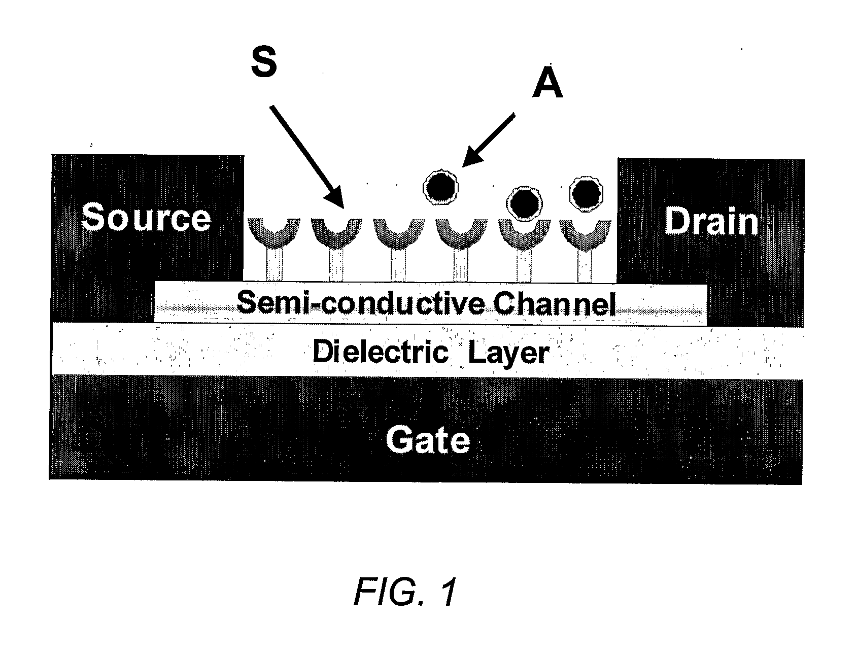
[0012]The invention is based in part on the unexpected finding that non-oxidized silicon nanowire-based sensors provide improved sensing capabilities. The lack of oxide layer on the surface of the nanowires improves the sensitivity of the detectors thus providing the detection of minute quantities of volatile organic compounds. The detection of minute quantities of volatile organic compounds enables the identification of biomarkers from body secretions without the need for pre-concentration.

Problems solved by technology

Consequently, real-time measurement of minute quantities of VOCs remains a challenge.
These factors include the need for expensive equipment, the degree of expertise required to operate such instruments, the length of time required to obtain data acquisition, and other technical problems in sampling, data analysis, etc.
This in turn lowers and consequently limits the effect of gate voltage on the transconductance of Si NW field effect transistors.
This limitation affects the response of sensors based on oxide-coated Si NW field effect transistors to their environment.
Yet, non-oxidized Si NWs as well as Si surfaces that are terminated with hydrogen tend to undergo oxidation upon exposure to ambient conditions, resulting in the formation of defects in the sensors.
However, exposure of these methyl-functionalized devices to analytes barely provides sensing responses, most probably due to the low ability of the methyl groups to adsorb vapor / liquid analytes.
Further modifications of the methyl functional groups for sensing applications at minute concentration down to the ppb levels, are not feasible.

Method used


Image

  • Chemically sensitive field effect transistors and uses thereof in electronic nose devices
  • Chemically sensitive field effect transistors and uses thereof in electronic nose devices
  • Chemically sensitive field effect transistors and uses thereof in electronic nose devices

Examples


example 1

Synthesis of the Silicon Nanowires (Si NWs)

[0095]Si NWs were prepared by the vapor-liquid-solid (VLS) growth method using chemical vapor deposition (CVD) with silane on Si(111) substrates. Si substrates were etched in diluted HF to remove the native oxide following by sputtering of a 2 nm thick Au film on the substrate. The sample was transferred into the CVD chamber, and annealed at ˜580° C. with a pressure of ˜5×10⁻⁷ mbar for 10 minutes. The temperature was then dropped to ˜520° C. and a mixture of 5-10 sccm Ar and 5 sccm SiH4 was introduced for 20 minutes at a pressure of 0.5-2 mbar to obtained undoped Si NWs. FIG. 3 shows a typical Scanning Electron Micrograph of Si NWs grown from gold (Au) seeds. FIG. 4 shows Transmission Electron Micrograph of the Si NWs in which the majority of the NWs exhibit smooth 50±10 nm diameter Si cores coated with 3-4 nm SiO2, having lengths in the range of 2-4 μm.

[0096]Doped Si NWs were prepared by the vapor-liquid-solid (VLS) growth technique under ...

example 2

Alkylation of Si Nanowires (Si NWs) Through Si—C Bond

[0097]Functionalization of the Si NWs of the present invention was performed using a two-step chlorination / alkylation route. Prior to any chemical treatment, each sample was cleaned using a nitrogen (N2(g)) flow. Hydrogen-terminated Si NWs were then prepared by etching the amorphous SiO2 coating. This was done through exposing the Si NWs to buffered HF solution (pH=5) for 60 seconds followed by exposure to NH4F for 30 seconds. It is noteworthy that longer exposures to HF and / or NH4F results in fluorination of the sample thus interfering with the alkylation process. The sample was then removed and rinsed in water for 2(g) flow for 10 seconds. The sample was transferred into a glove-box with N2(g)-atmosphere for functionalization.

[0098]Functionalization was preformed by immersing the sample into a saturated solution of PCl5 in C6H5Cl (0.65M) that contained a few grains of C6H5OOC6H5 to act as a radical initiator (Hassler and Koell, ...

example 3

The Kinetics of Formation of Functionalized Si NWs

[0099]The coverage of Si NW surfaces with various alkyl chains was plotted as a function of time. FIG. 6 shows a semi-logarithmic plot from which the pseudo-first-order rate constant of the reaction was calculated. Two distinct regions are observed in the curves: at short time intervals an accelerated rate is obtained (corresponds to a Kp1 slope) and at longer time intervals mildly increased rate is obtained (corresponds to a Kp2 slope). Without being bound by any theory or mechanism of action, the increased rate is attributed to the lack of steric hindrance between adjacent alkyl chains. This result is compatible with the kinetics of a pseudo-first-order reaction.

[0100]The kinetics of pseudo first order (ln [n]=−Kp1*t) is detected for up to about 90% of a full coverage of the Si NWs followed by a decrease in rate thereafter. The two main regions in the alkylation process of the NWs are from zero to Γsat, and from Γsat to longer alky...


PUM


Abstract

The present invention provides an electronic nose device based on chemically sensitive field effect transistors. In particular, the sensors of the electronic nose device are composed of non-oxidized, functionalized silicon nanowires which can detect volatile organic compounds with very high sensitivity. Methods of use in diagnosing diseases including various types of cancer are disclosed.

Description

FIELD OF THE INVENTION[0001]The present invention relates to an electronic device for detecting volatile organic compounds with high sensitivity. In particular, the present invention provides chemically sensitive field effect transistors of non-oxidized, functionalized silicon nanowires and methods of use thereof.BACKGROUND OF THE INVENTION[0002]Electronic nose devices perform odor detection through the use of an array of cross-reactive sensors in conjunction with pattern recognition methods. In contrast to the “lock-and-key” model, each sensor in the electronic nose device is widely responsive to a variety of odorants. In this architecture, each analyte produces a distinct signature from the array of broadly cross-reactive sensors. This configuration allows to considerably widen the variety of compounds to which a given matrix is sensitive, to increase the degree of component identification and, in specific cases, to perform an analysis of individual components in complex multi-com...

Claims


Application Information

Patent Timeline
IPC IPC(8): G06F19/00H01L29/66G01N33/48G06F15/18G06N3/02G06N3/12G06N5/04G06N7/04
CPCB82Y15/00G01N27/4146G01N2033/4975G01N33/0034G01N33/4975H01L29/0843B82Y30/00G01N33/54373Y10S977/742G01N27/4148Y10S977/70H01L29/772
Inventor HAICK, HOSSAM
Owner TECHNION RES & DEV FOUND LTD
Learn More