Method for fabricating a semiconductor chip device having through-silicon-via (TSV)
a technology of throughsilicon and semiconductor chips, applied in semiconductor devices, semiconductor/solid-state device details, electrical apparatus, etc., can solve the problems of low yield and cost, easy filling, unstable process, etc., and achieve high-density connection, save fabrication costs, and simplify fabrication methods
- Summary
- Abstract
- Description
- Claims
- Application Information
AI Technical Summary
Benefits of technology
Problems solved by technology
Method used
Image
Examples
first embodiment
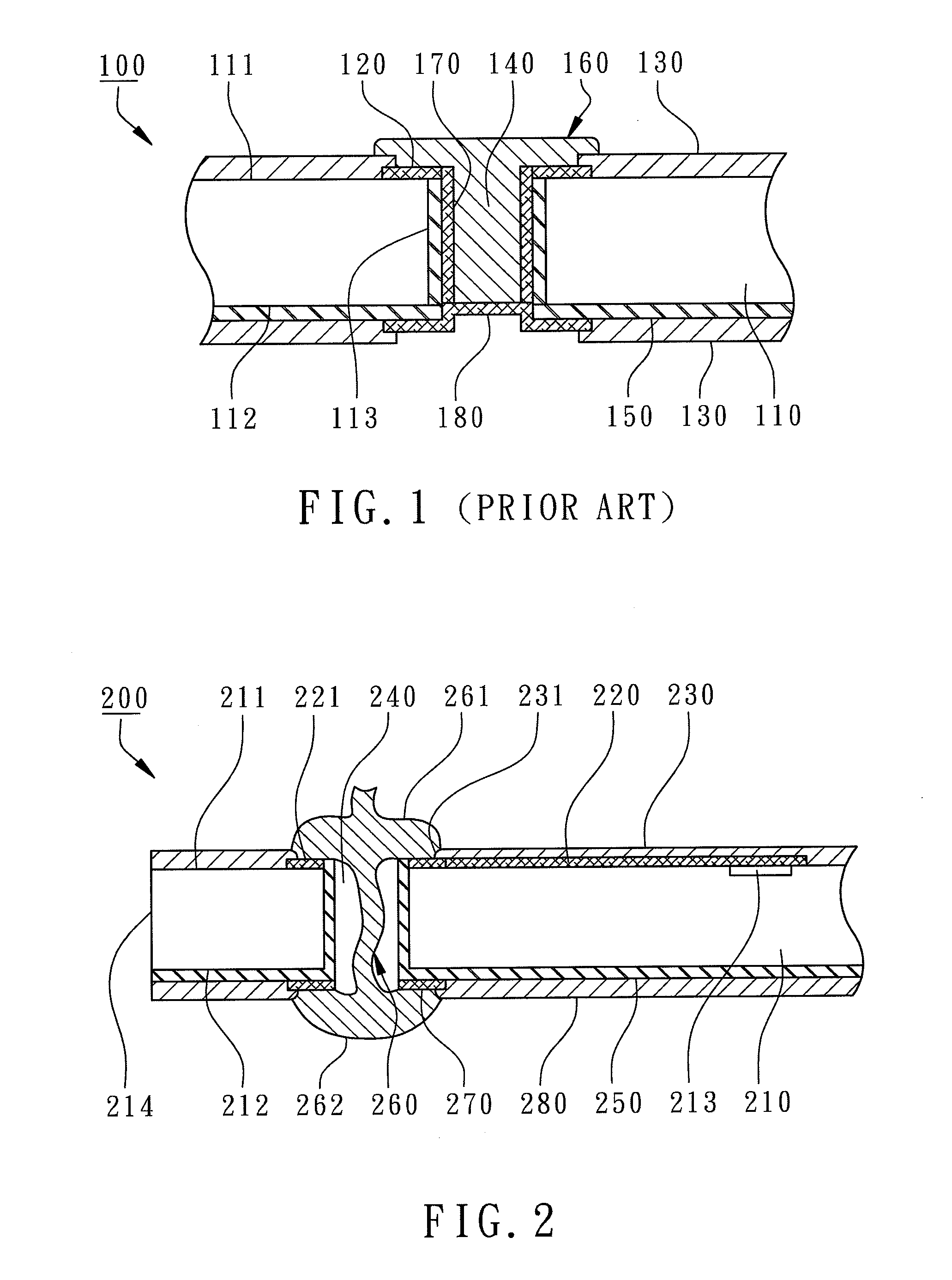
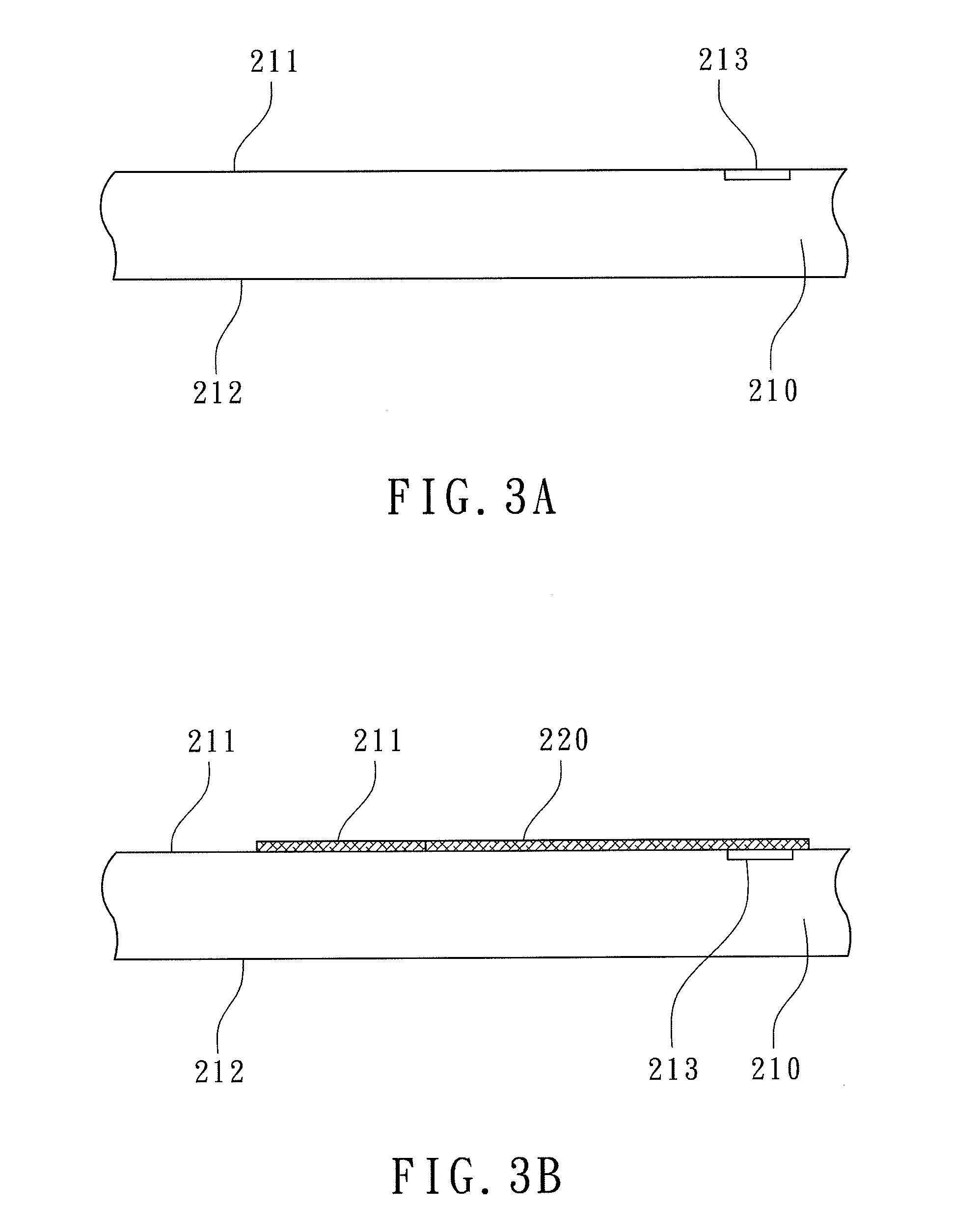
[0016]According to the present invention as shown in FIG. 2, a semiconductor device 200 with TSV primarily comprises a first chip 210, a redistributed trace layer 220, a first passivation layer 230, a plurality of through holes 240, an insulation layer 250, and a plurality of flexible metal wires 260. The chip 210 has an active surface 211, a back surface 212, and a plurality of bonding pads 213 formed on the active surface 211. Therein, only one of the through holes 240, one of the metal wires 260 and one of the bonding pads 213 are shown in FIG. 2. A variety of integrated circuits (IC) are formed on the active surface 211 and are electrically connected to the bonding pads 213. The material of the chip can be Si, GaAs, or other semiconductor materials.
[0017]The redistributed trace layer 220 is electrically conductive and is disposed on the active surface 211. The redistributed trace layer 220 includes a plurality of redistributed pads 221 electrically connected to the bonding pads ...
second embodiment
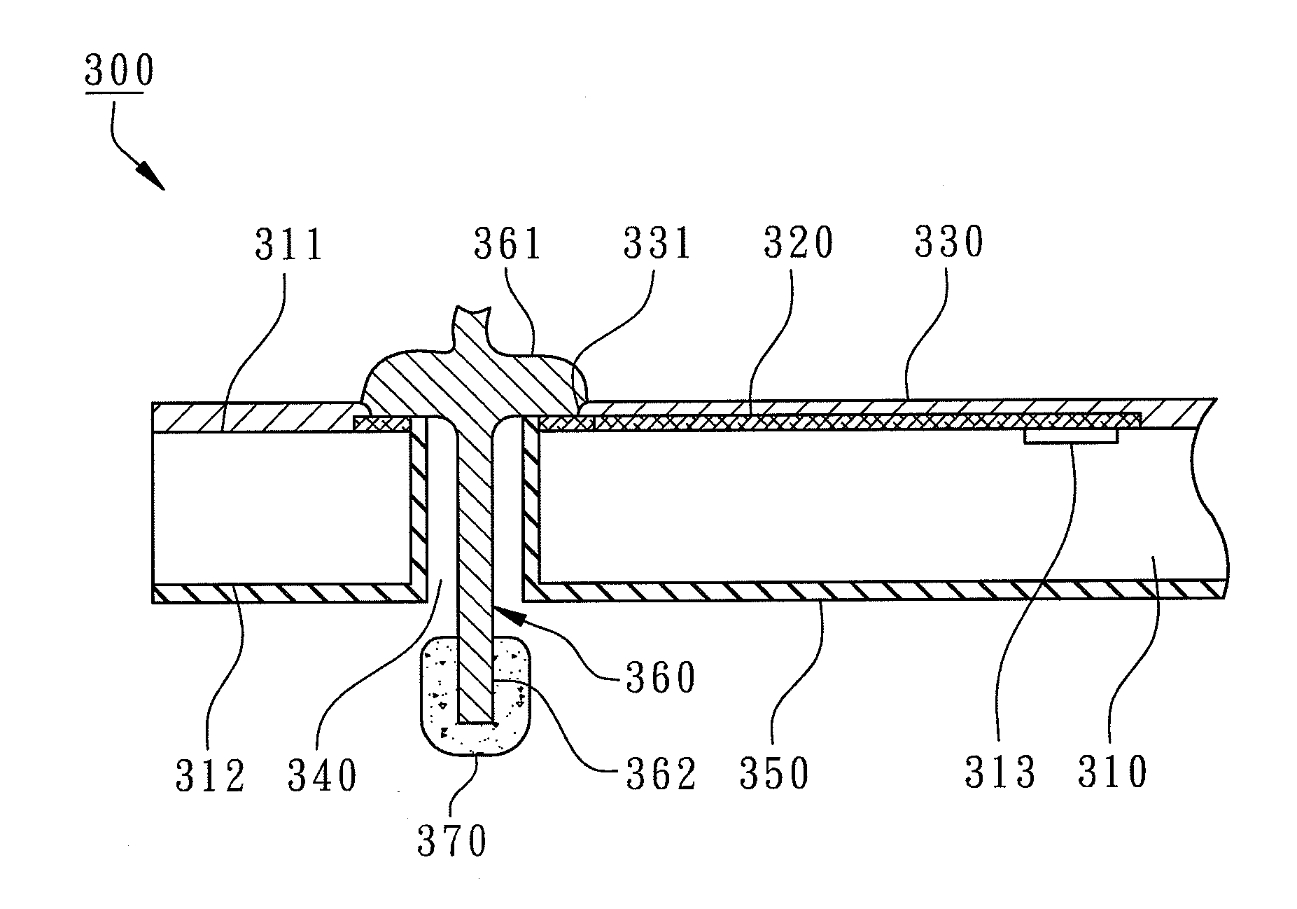
[0033]In the present invention, as shown in FIG. 6, another semiconductor device with TSV is revealed. The semiconductor device 300 primarily comprises a chip 310, a redistributed trace layer 320, a passivation layer 330, a plurality of through holes 340, an insulation layer 350, and a plurality of flexible metal wires 360. The chip 310 has an active surface 311, a back surface 312, and a plurality of bonding pads 313 formed on the active surface 311. The redistributed trace layer 320 is formed on the active surface 311 and includes a plurality of redistributed pads 321 electrically connected to the bonding pads 313. The passivation layer 330 is formed over the active surface 311 of the chip 310 to cover the redistributed trace layer 320. The passivation layer 330 further has a plurality of openings 331 to expose the corresponding redistributed pads 321 for bonding the flexible metal wires 360.
[0034]The though holes 340 are formed through the corresponding redistributed pads 321 and...
PUM
 Abstract
Description
Claims
Application Information
 - R&D
- Intellectual Property
- Life Sciences
- Materials
- Tech Scout
- Unparalleled Data Quality
- Higher Quality Content
- 60% Fewer Hallucinations
Browse by: Latest US Patents, China's latest patents, Technical Efficacy Thesaurus, Application Domain, Technology Topic, Popular Technical Reports.
© 2025 PatSnap. All rights reserved.Legal|Privacy policy|Modern Slavery Act Transparency Statement|Sitemap|About US| Contact US: help@patsnap.com


