
Pulsed selective area lateral epitaxy for growth of iii-nitride materials over non-polar and semi-polar substrates

a lateral epitaxy and selective area technology, applied in the direction of crystal growth process, polycrystalline material growth, chemically reactive gas growth, etc., can solve the problems of segregation of electrons and holes to opposite faces, generation of basal stacking faults, and further charge separation within quantum heterostructures

Active Publication Date: 2010-06-10
UNIVERSITY OF SOUTH CAROLINA
View PDF11 Cites 264 Cited by
  • Summary
  • Abstract
  • Description
  • Claims
  • Application Information

AI Technical Summary

Benefits of technology

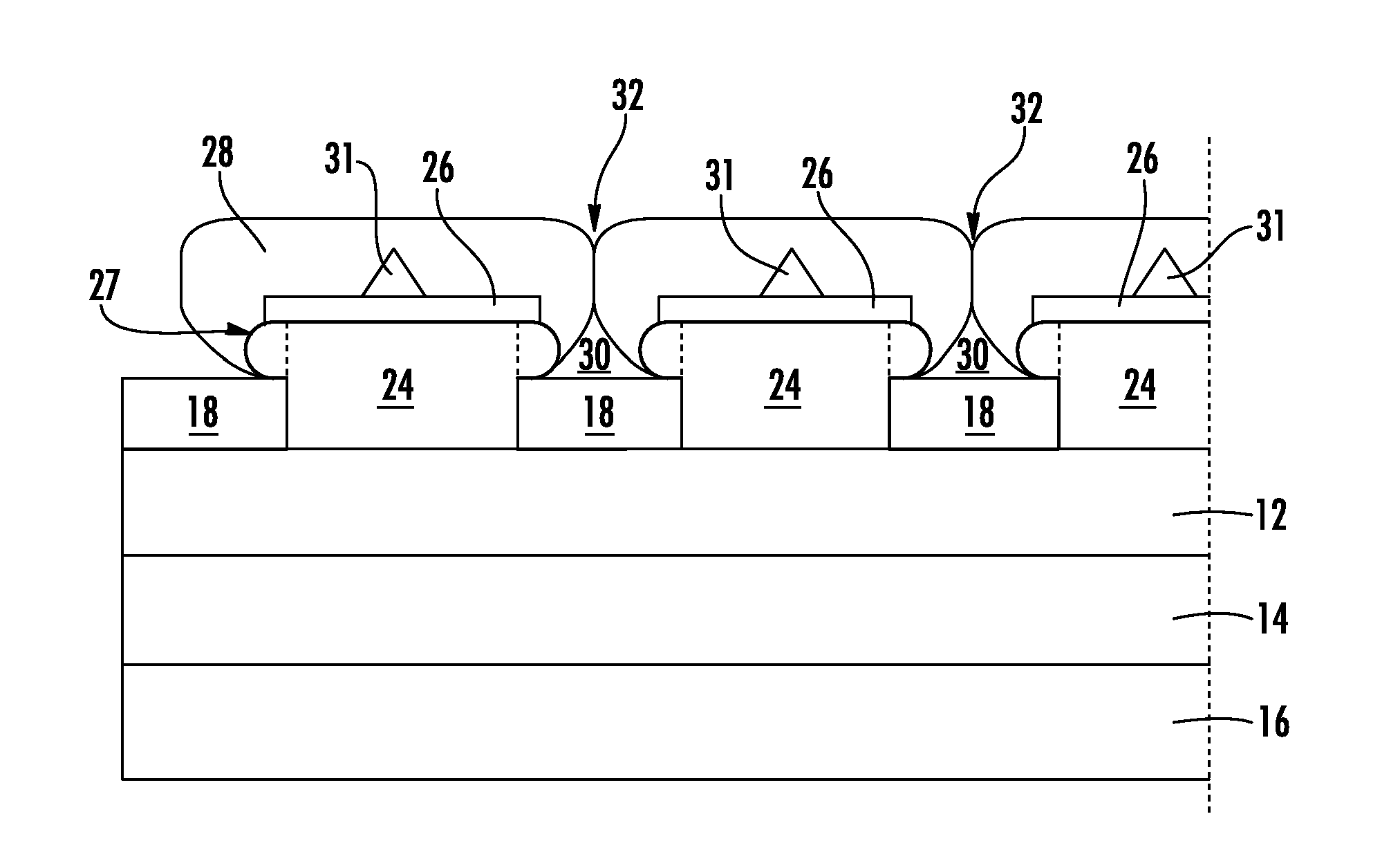
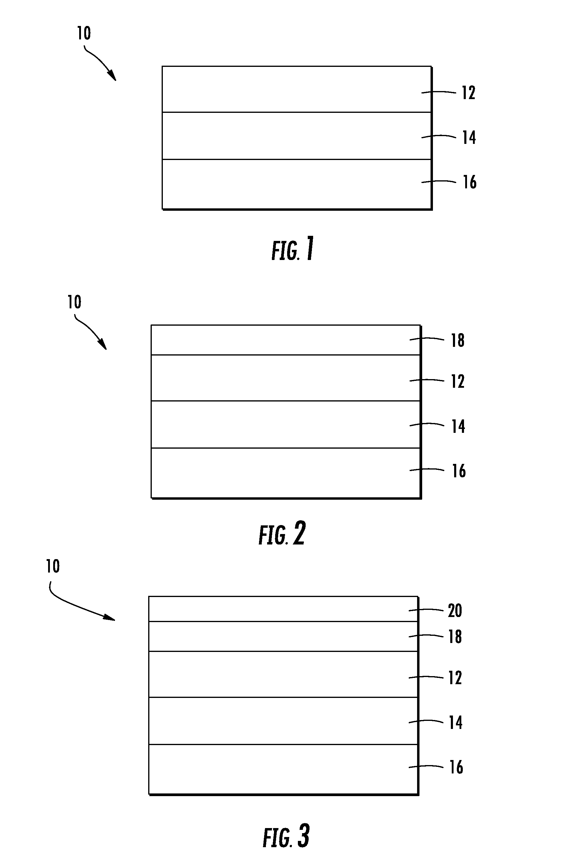
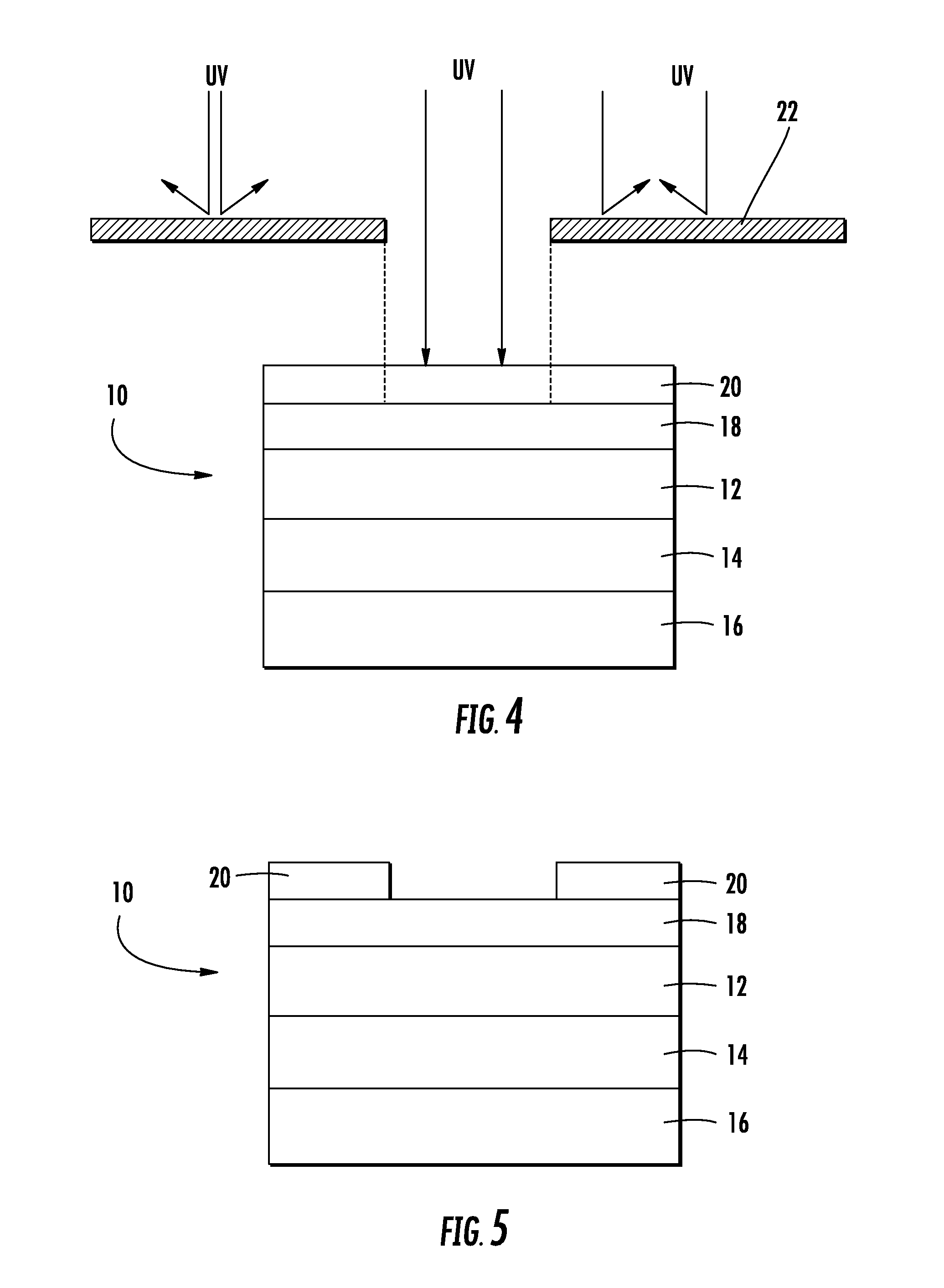
The present invention is about a method of growing a non-polar or semi-polar group III nitride layer on a base layer. The method involves masking the base layer with a first dielectric layer, growing a mushroom-shaped PLOG group III nitride layer on the exposed areas of the base layer, masking the mushroom-shaped PLOG group III nitride layer with a second dielectric layer, and growing a non-polar or semi-polar group III nitride layer from each exposed side of the mushroom-shaped PLOG group III nitride layer. The technical effect of this invention is to provide a method for growing high-quality non-polar or semi-polar group III nitride layers on a base layer, which can be useful in various applications such as light-emitting diodes and laser diodes.

Problems solved by technology

A negative consequence of this growth direction is that each layer material will suffer from segregation of electrons and holes to opposite faces of the layers due to the spontaneous polarization of the crystal.
Furthermore, strain at the interfaces between adjacent layers gives rise to piezoelectric polarization, causing further charge separation within quantum heterostructures.
However, when non-polar III-Nitride layers are deposited on sapphire substrates, threading dislocations, as well as basal stacking faults, are generated due to lattice mismatch.
This adduct formation during MOCVD also hampers the subsequent epilayer growths by increasing the number of stacking faults and dislocation density.
Although the P-MOCVD alleviates some of the potential problems plaguing III-N devices (especially over non-polar substrates and materials) and represents an enabling technology for the growth of non-polar III-N devices, the relatively high defect density in the directly-grown non-polar or semi-polar III-N films reduces the efficiency of subsequently grown devices compared to what could be achieved by homoepitaxial growth on a perfect substrate.
This high temperature then subsequently brings in additional problems such as material decomposition, mask auto-doping etc.

Method used


Image

  • Pulsed selective area lateral epitaxy for growth of iii-nitride materials over non-polar and semi-polar substrates
  • Pulsed selective area lateral epitaxy for growth of iii-nitride materials over non-polar and semi-polar substrates
  • Pulsed selective area lateral epitaxy for growth of iii-nitride materials over non-polar and semi-polar substrates

Examples


example 1

[0083]A 1.5 μm thick a-plane GaN films was deposited over r-plane sapphire substrates using pulse atomic layer epitaxy (PALE). The growth temperature was 990C and growth pressure was 40 torr. Tri-ethyl gallium and ammonia were used the precursors for pulse atomic layer epitaxy of GaN. By adjusting the pulse condition including the pulse time (0-100 secs), ramping time (0-100 secs), total flow of triethyl gallium (5-500 sccm) and ammonia (1-30 SLM), smooth GaN was achieved. The basal stacking faults seen in conventional MOCVD as seen in FIG. 15(a) are significantly reduced by using pulse atomic layer epitaxy shown in FIG. 15(b).

[0084]Selective area growth of GaN was carried out over a digital dielectric deposited SiO2 mask using pulse selective area lateral epitaxy method. The geometrical parameters of the obtained structure were studied using scanning electron microscope (SEM). The SiO2 stripe openings were 5 μm and the period was 15 μm. The openings were oriented along [1-100]. In ...


PUM

PropertyMeasurementUnit
RF poweraaaaaaaaaa
thicknessaaaaaaaaaa
thicknessaaaaaaaaaa

Abstract

An epitaxy procedure for growing extremely low defect density non-polar and semi-polar III-nitride layers over a base layer, and the resulting structures, is generally described. In particular, a pulsed selective area lateral overgrowth of a group III nitride layer can be achieved on a non-polar and semi-polar base layer. By utilizing the novel P-MOCVD or PALE and lateral over growth over selected area, very high lateral growth conditions can be achieved at relatively lower growth temperature which does not affect the III-N surfaces.

Description

PRIORITY INFORMATION[0001]The present application claims priority to U.S. Provisional Patent Application No. 60 / 875,009 filed on Dec. 15, 2006, naming Asif Khan, Qhalid Fareed, and Vinod Adivarahan as inventors, which is incorporated by reference herein in its entirety.GOVERNMENT SUPPORT CLAUSE[0002]The present invention was developed with funding from the U.S. Army Space and Missile Defense Command under contract no. DASG60-02-1-0002. The government retains certain rights in the invention.BACKGROUND OF THE INVENTION[0003]Group III-nitride and its ternary and quaternary compounds are prime candidates for fabrication of visible and ultraviolet high-power and high-performance optoelectronic devices and electronic devices. These devices are typically grown epitaxially as thin films by growth techniques including molecular beam epitaxy (MBE), metalorganic chemical vapor deposition (MOCVD), or hydride vapor phase epitaxy (HVPE). The selection of substrates is critical for determining the...

Claims


Application Information

Patent Timeline
Patent Type & Authority Applications(United States)
IPC IPC(8): H01L29/20C30B25/04
CPCC30B25/04C30B29/403H01L21/02389H01L21/0242H01L21/02647H01L21/02458H01L21/0254H01L21/0262H01L21/02433
Inventor KHAN, M. ASIFADIVARAHAN, VINOD
Owner UNIVERSITY OF SOUTH CAROLINA
Learn More