
Well-Structure Anti-Punch-through Microwire Device

a microwire and well-structure technology, applied in the field of integrated circuit (ic) fabrication, can solve the problems of poor wire diameter and length uniformity, adjacent wires only partially depleted, wires to be fully depleted, etc., and achieve the effect of greater yield, greater uniformity, and more growth conditions

Inactive Publication Date: 2010-03-25
SHARP KK
View PDF12 Cites 10 Cited by
  • Summary
  • Abstract
  • Description
  • Claims
  • Application Information

AI Technical Summary

Benefits of technology

[0007]A microwire architecture is disclosed herein that permits the use of larger diameter wires having a fully-doped, modulated P-N-P, or N-P-N structure with an intrinsic epitaxial Si shell for NMOS or PMOS transistor applications. The use of larger diameters (dwire>500 nm) is desirable for a number of reasons. First, growth conditions are more favorable for larger diameter wires—providing a higher yield and greater uniformity. The use of an epitaxial intrinsic Si layer permits a finer control of the depletion region, so the devices can become fully depleted, enabling better control of the device parameters (e.g., threshold voltage) and uniformity. The modulated doping transient lengths (i.e., the growth length between when the source / drain dopant is on and off) have less impact on the overall device performance. The use of an epitaxial Si layer for the channel also permits precise threshold voltage adjustments to be made independent of the modulated growth process.
[0008]Further, the effective channel width scales with the diameter, so that a 1 μm microwire has a channel width 10 times that of conventional nanowires with a typical diameter of approximately 100 nanometers (nm). Larger channel widths permit higher Ion per wire and reduce the need for multiple wires to be deposited per device.
[0009]Accordingly, a method is provided for fabricating a well-structure anti-punch-through microwire device. The method initially forms a microwire with alternating highly and lightly doped cylindrical regions. A channel ring is formed surrounding a first dopant well-structure region in the microwire, between source and drain (S / D) regions of the microwire. The S / D regions are doped with a second dopant, opposite to the first dopant. A gate dielectric ring is formed surrounding the channel ring, and a gate electrode ring is formed surrounding the gate dielectric ring. The well-structure, in contrast to conventional micro or nanowire transistors, helps prevent the punch-through phenomena. In one aspect, the channel ring is formed external to the microwire outer shell wall.

Problems solved by technology

However, there are several problems associated with these wires, such as the ability to control the dopant concentration and width of the intrinsic channel, poor wire diameter and length uniformity, and harvesting of the nanowires (NWs) for dispersion onto a larger substrate.
The NW wire diameter can affect the depth of the depletion layer within the transistor channel, and poor uniformity can cause some wires to be fully depleted, with adjacent wires only partially depleted.
This is especially problematic for the control of threshold voltage distribution.

Method used


Image

  • Well-Structure Anti-Punch-through Microwire Device
  • Well-Structure Anti-Punch-through Microwire Device
  • Well-Structure Anti-Punch-through Microwire Device

Examples


Embodiment Construction

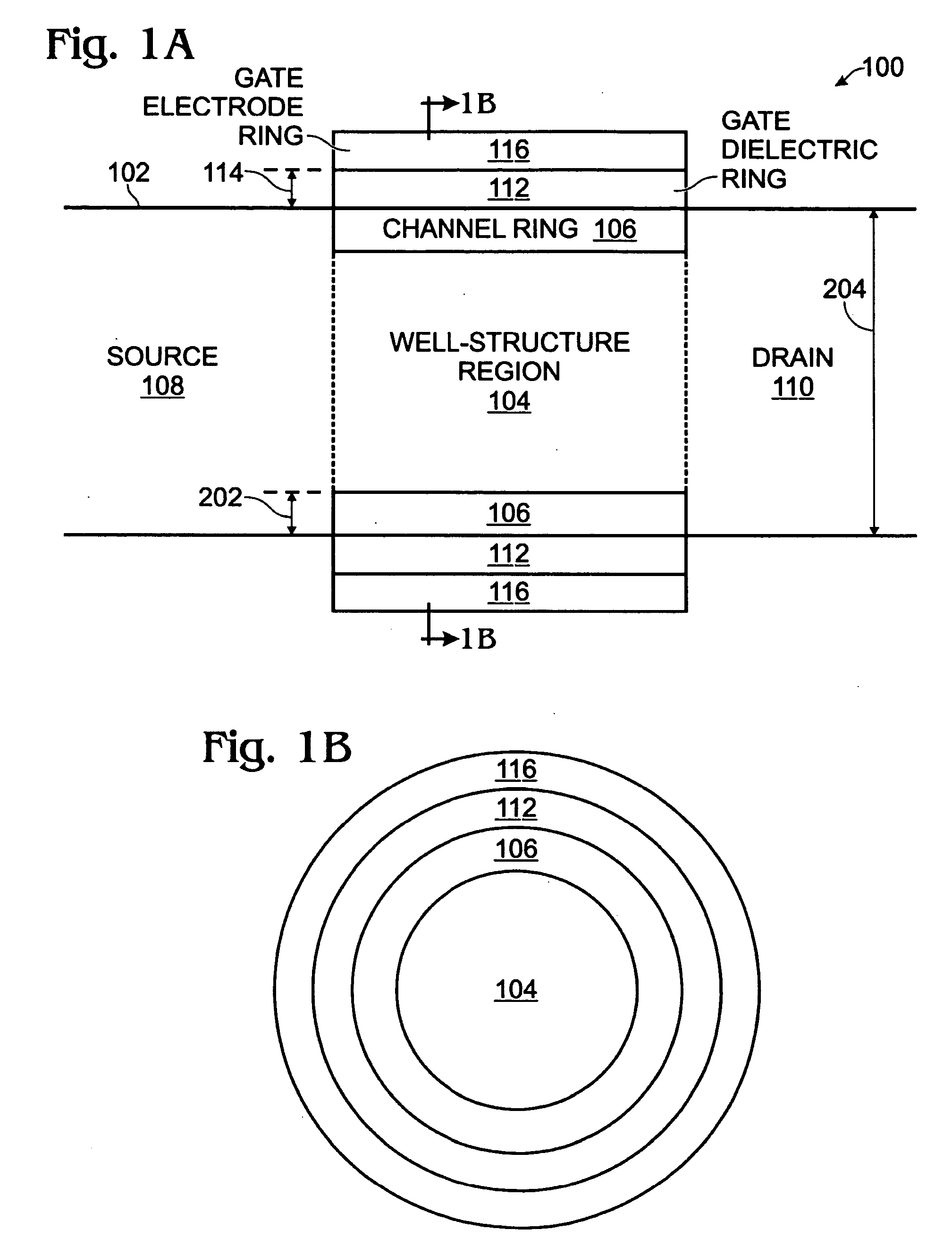
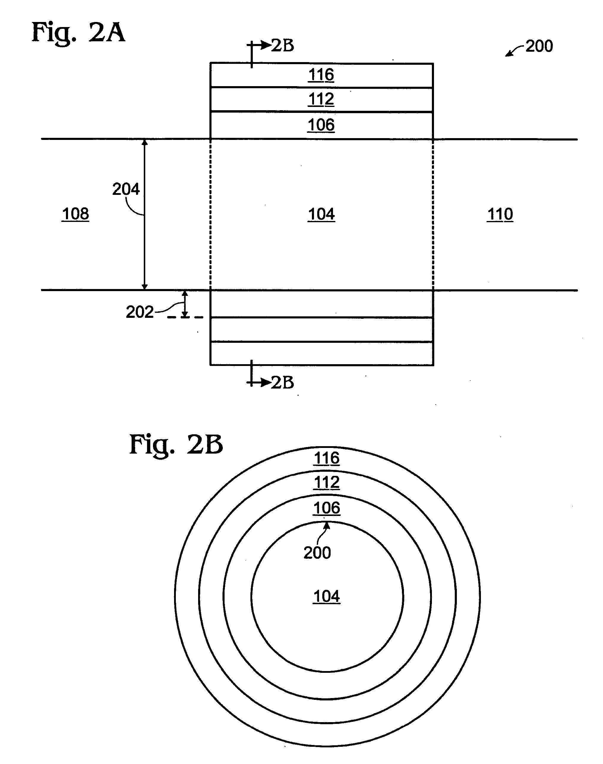
[0020]FIGS. 1A and 1B are partial cross-sectional views of a well-structure anti-punch-through microwire device. The device 100 comprises a microwire 102 with alternating highly and lightly doped cylindrical regions, including a first dopant well-structure region 104. A channel ring 106 surrounds the well-structure region 104, between source 108 and drain 110 regions of the microwire. The source and drain (S / D) regions 108 / 110 are doped with a second dopant, opposite to the first dopant. For example, the first dopant may be n-type and the second dopant p-type. Alternately, the first dopant may be p-type and first dopant n-type. Thus, the microwire alternating highly and lightly doped cylindrical regions are either an NPN or PNP sequence.

[0021]A gate dielectric ring 112 overlies the channel ring 106. Typically, the gate dielectric ring 112 has a ring thickness 114 in the range of 10 to 60 nm. A gate electrode ring 116 overlies the gate dielectric ring 112.

[0022]FIGS. 2A and 2B are pa...


PUM


Abstract

A well-structure anti-punch-through microwire device and associated fabrication method are provided. The method initially forms a microwire with alternating highly and lightly doped cylindrical regions. A channel ring is formed external to the microwire outer shell and surrounding a first dopant well-structure region in the microwire, between source and drain (S / D) regions of the microwire. The S / D regions are doped with a second dopant, opposite to the first dopant. A gate dielectric ring is formed surrounding the channel ring, and a gate electrode ring is formed surrounding the gate dielectric ring. The well-structure, in contrast to conventional micro or nanowire transistors, helps prevent the punch-through phenomena.

Description

BACKGROUND OF THE INVENTION[0001]1. Field of the Invention[0002]This invention generally relates to integrated circuit (IC) fabrication and, more particularly, to a well-structure microwire transistor device.[0003]2. Description of the Related Art[0004]As-grown, in-situ end-doped core-shell-shell (ECSS) nanowires are known for use in the fabrication of transistor devices. However, there are several problems associated with these wires, such as the ability to control the dopant concentration and width of the intrinsic channel, poor wire diameter and length uniformity, and harvesting of the nanowires (NWs) for dispersion onto a larger substrate.[0005]The NW wire diameter can affect the depth of the depletion layer within the transistor channel, and poor uniformity can cause some wires to be fully depleted, with adjacent wires only partially depleted. This is especially problematic for the control of threshold voltage distribution.[0006]It would be advantageous if the performance of NW...

Claims


Application Information

Patent Timeline
IPC IPC(8): H01L21/336H01L29/78
CPCB82Y10/00H01L29/0673H01L29/78H01L29/068H01L29/125H01L29/0676Y10S977/936
Inventor CROWDER, MARK ALBERT
Owner SHARP KK
Learn More