Method of forming barrier film

Active Publication Date: 2010-03-18
ULVAC INC
View PDF3 Cites 280 Cited by
  • Summary
  • Abstract
  • Description
  • Claims
  • Application Information

AI Technical Summary

Benefits of technology

[0020]Thus the present invention performs adsorption and modification steps at low temperature using ALD in a coating apparatus provided with microwave-excited plasma generation means, resulting the advantage that the formed barrier film fully and closely covers high aspect ratio fine holes, trenches, etc. without any overhang above these features.BEST MODES OF CARRYING OUT THE INVENTION
[0021]There will first be described a first coating apparatus used in a method of forming a film according to the present invention. The first coating apparatus includes a vacuum chamber having at its bottom portion a stage for mounting an object to be coated thereon, and also includes a shower head structure provided at the ceiling of the vacuum chamber and facing the object to be coated. This shower head structure will now be described in detail with reference to FIG. 1.
[0022]The shower head structure 1 includes a coaxial resonant cavity 11 provided at its top portion, a reactive gas introduction chamber 12 connected to the bottom portion of the coaxial resonant cavity 11, and a shower head unit 13 connected to the reactive gas introduction chamber 12.
[0023]The coaxial resonant cavity 11 is made of, e.g., copper or aluminum, and a nonmetallic pipe 111 penetrates through the ceiling and bottom walls of the cavity. The top portion of the nonmetallic pipe 111 is connected through flow rate control means to a reactive gas source, not shown. The nonmetallic pipe 111 may be a quartz, sapphire, or aluminum tube. However, it is preferably a sapphire or aluminum tube to reduce particles.
[0024]An upper conductor 112 is movably and concentrically mounted around the upper portion of this nonmetallic pipe 111 and covers the periphery of that portion. The bottom wall of the coaxial resonant cavity 11 below the upper conductor 112 serves as a lower conductor 113. The portion of the nonmetallic pipe 111 between these two conductors is exposed, and this exposed portion, 111a, is irradiated with a microwave. It should be noted that although in FIG. 1 the bottom wall of the coaxial resonant cavity 11 is shown to serve as the lower conductor 113, it is to be understood that another member may be mounted on the bottom portion of the coaxial resonant cavity 11 and used as the lower conductor 113.
[0025]To generate plasma in the region inside the exposed portion 111a of the nonmetallic pipe 111, microwave supply means 14 is mounted on the sidewall of the coaxial resonant cavity 111 at a position corresponding to that of the exposed portion 111a. This microwave supply means 14 includes: a magnetron 141 for generating a microwave; a microwave power supply 142 for powering the magnetron 141; an antenna 143 connected to the magnetron 141 to apply the microwave generated by the magnetron 141 at a resonant frequency (e.g., 2.45 GHz) to the coaxial resonant cavity 11; and a coaxial cable 144 connected between the antenna 143 and the magnetron 141. When the microwave power supply 142 is activated, the magnetron 141 generates a microwave, which passes through the coaxial cable 144 to the antenna 143 mounted at the wall surface. When this microwave is transmitted within the coaxial resonant cavity 11 through the antenna 143, the reactive gas that has been introduced into the top portion of the nonmetallic pipe 111 and has reached the region in the exposed portion 111a is converted into a plasma state and this plasma gas is delivered into the reactive gas introduction chamber 12 through the lower portion of the nonmetallic pipe 111, which portion serves as a gas flow path. Thus, this apparatus does not include a waveguide for propagating the microwave. This means that the generation of the microwave quickly results in generation of plasma, making the apparatus suitable for ALD. Although in FIG. 1 only one antenna 143 is shown, it is to be understood that two or more antennas may be used. Further, since, as described above, the upper conductor 112 is movable, its position may be varied to vary the electric field generated between the upper and lower conductors 112 and 113 and thereby vary the conditions under which the plasma is generated.

Problems solved by technology

However, these buried wiring structures are disadvantageous in that when the main wiring material is, e.g., Cu, it tends to diffuse into the insulating film, thereby causing problems.
However, in order to form a good ZrB2 film, this method requires that the substrate be heated to 550° C. or more, which is not desirable.

Method used


Image

  • Method of forming barrier film
  • Method of forming barrier film
  • Method of forming barrier film

Examples


example 1

Practical Example 1

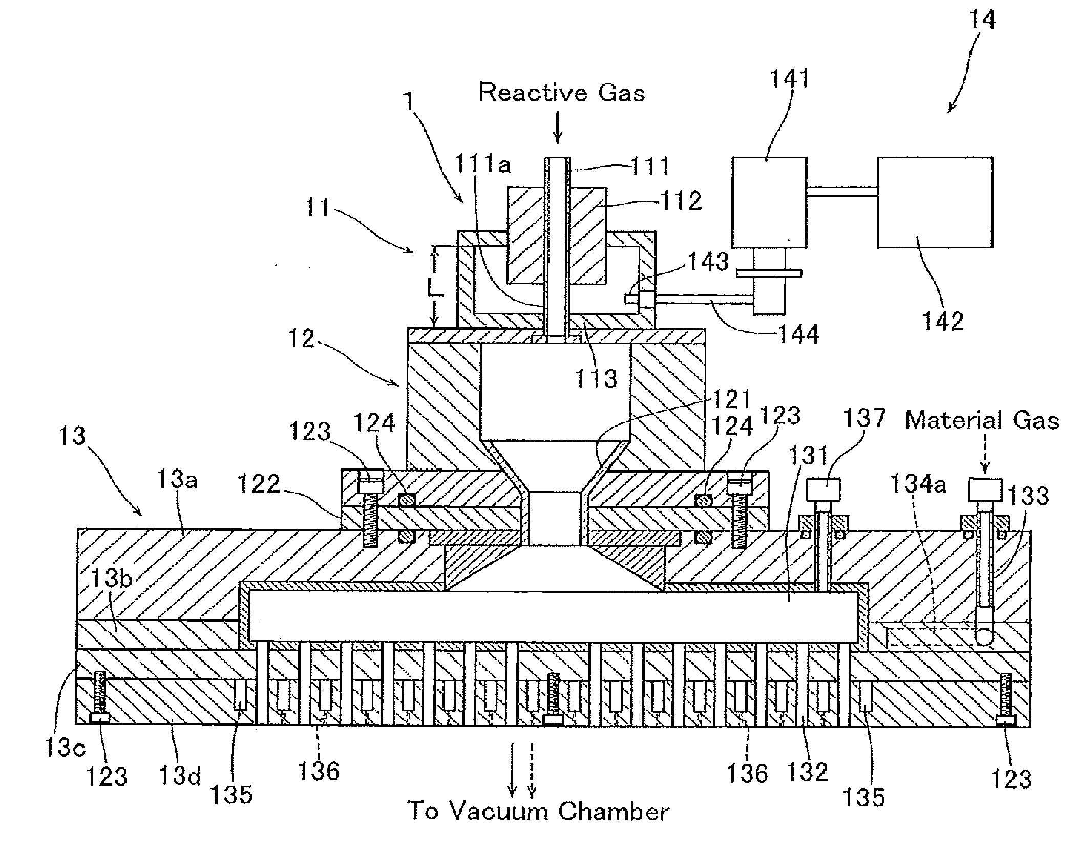
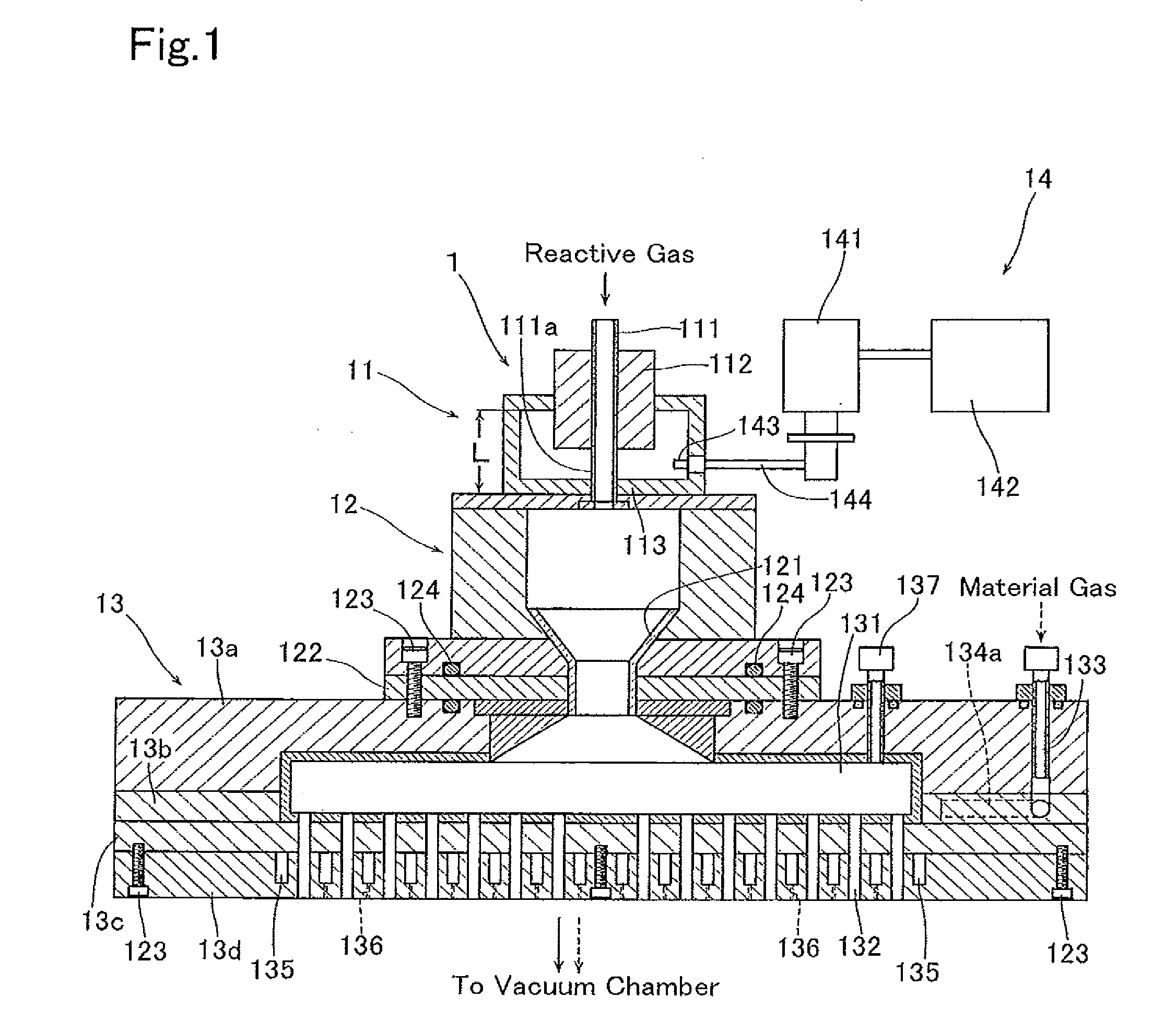
[0084]In this example, a film was formed in the first coating apparatus using the process sequence shown in FIG. 6. The parameters in the adsorption step were set as follows: time=5 sec; flow rate of reactive gas (H2 gas)=100 sccm; flow rate of bubbling gas (Ar) for material gas [Zr(BH4)4 gas]=100 sccm; and evacuation rate=1000 L / sec. The parameters in the modification step were set as follows: time=25 sec; reactive gas flow rate=100 sccm; microwave input power=0.5 kW; and evacuation rate=1000 L / sec. These adsorption and modification steps were each repeated 24 times to form a film on a substrate S. The resultant film was a ZrB2 film having a thickness of 10 μm.

example 2

Practical Example 2

[0085]In this example, a film was formed in the first coating apparatus using the process sequence shown in FIG. 9. The parameters in the adsorption step were set as follows: time=5 sec; flow rate of reactive gas (H2 gas)=100 sccm; flow rate of bubbling gas (Ar) for material gas [Zr(BH4)4 gas]=100 sccm; microwave input power=0.5 kW; and evacuation rate=1000 L / sec. The parameters in the modification step were set as follows: time=25 sec; reactive gas flow rate=100 sccm; microwave input power=0.5 kW; and evacuation rate=1000 L / sec. These adsorption and modification steps were each repeated 24 times to form a film on a substrate S. The resultant film was a ZrB2 film having a thickness of 10 μm.

example 3

Practical Example 3

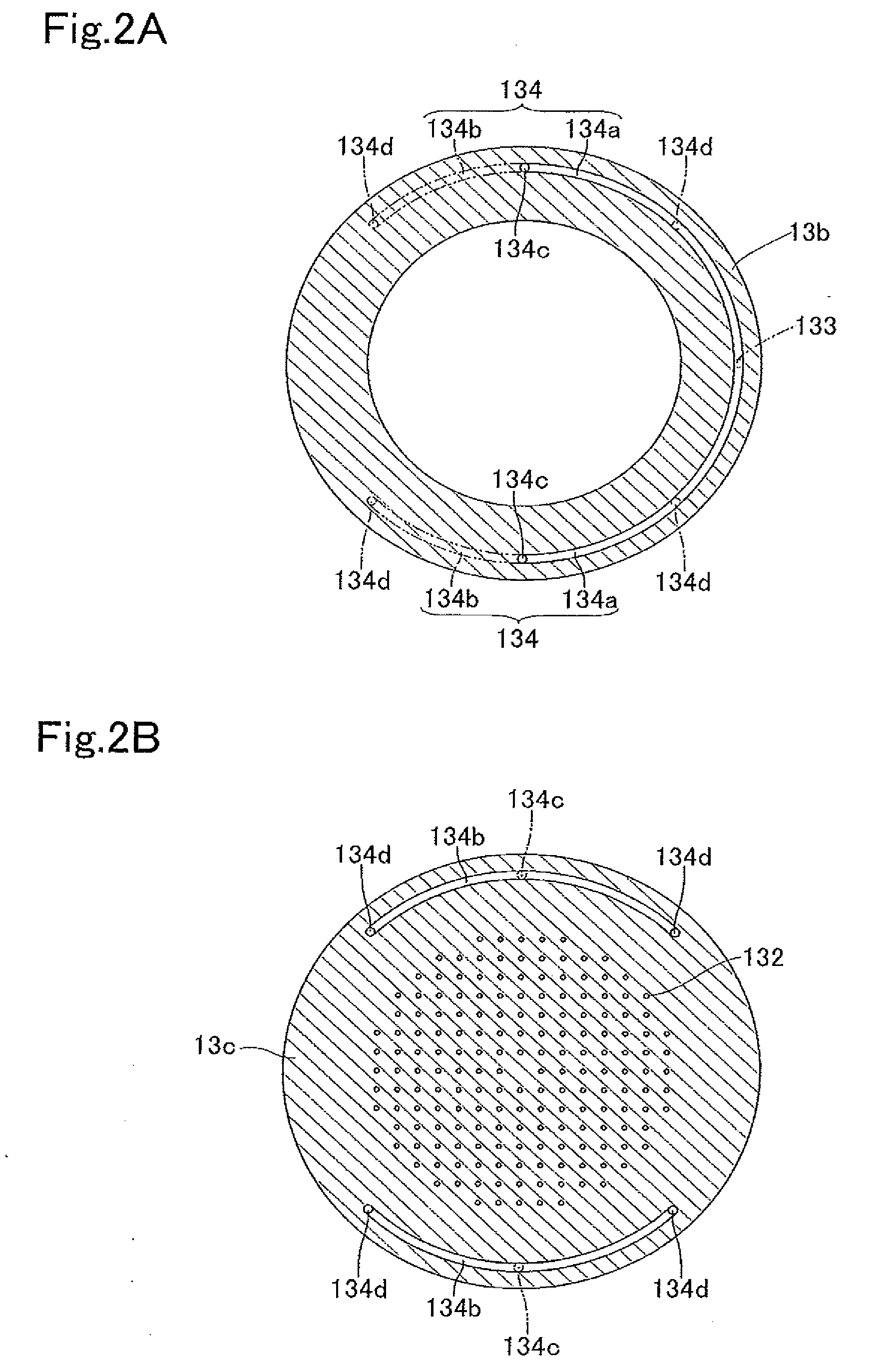
[0086]In this example, a film was formed in the second coating apparatus using the process sequence shown in FIG. 6. The parameters in the adsorption step were set as follows: time=5 sec; flow rate of reactive gas (H2 gas)=100 sccm; flow rate of bubbling gas (Ar) for material gas [Zr(BH4)4 gas]=100 sccm; and evacuation rate=1000 L / sec. The parameters in the modification step were set as follows: time=25 sec; reactive gas flow rate=100 sccm; microwave input power=0.5 kW; and evacuation rate=1000 L / sec. These adsorption and modification steps were each repeated 24 times to form a film on a substrate S. Further, the inside of the coaxial resonant cavity 11 and the double pipe 22 were cooled during this deposition process. The resultant film was a ZrB2 film having a thickness of 10 μm, and etching of the inner surface of the gas passage 227, such as that shown in FIG. 12, was prevented.


PUM

PropertyMeasurementUnit
Temperatureaaaaaaaaaa
Flow rateaaaaaaaaaa
Heightaaaaaaaaaa

Abstract

A barrier film made of a ZrB2 film is formed by use of a coating apparatus provided with plasma generation means including a coaxial resonant cavity and a microwave supply circuit for exciting the coaxial resonant cavity, the coaxial resonant cavity including spaced apart conductors provided around the periphery of a nonmetallic pipe for reactive gas introduction, the coaxial resonant cavity having an inner height equal to an integer multiple of one-half of the exciting wavelength, the plasma generation means being constructed such that a gas injected from one end of the nonmetallic pipe is excited into a plasma state by a microwave when the gas is in a region of the nonmetallic pipe which is not covered with the conductors and such that the gas in the plasma state is discharged from the other end of the nonmetallic pipe.

Description

TECHNICAL FIELD[0001]The present invention relates to a method of forming a barrier film.BACKGROUND ART[0002]With the scaling down of patterns of semiconductor integrated circuits, there have recently been proposed so-called “buried wiring structures,” in which fine contact holes, trenches, etc. having a high aspect radio are buried with a wiring material such as Cu or Al.[0003]However, these buried wiring structures are disadvantageous in that when the main wiring material is, e.g., Cu, it tends to diffuse into the insulating film, thereby causing problems. Therefore, a conductive barrier film is provided between the insulating film and the wiring material to limit or prevent diffusion of Cu. Various methods of forming this barrier film have been proposed. For example, one known method is to deposit a material layer of Ta, TiN, TaN, etc. using PVD, MOCVD, or ALD to form a barrier film (see, e.g., Patent Document 1) .[0004]ALD is a technique of forming a desired metal film by first ...

Claims


Application Information

Patent Timeline
IPC IPC(8): H01L21/46
CPCC23C16/30C23C16/38C23C16/4554H01L21/76843C23C16/45565H01L21/28562C23C16/45555H01L21/28H01L21/285
Inventor HATANAKA, MASANOBUISHIKAWA, MICHIOTSUMAGARI, KANAKO
Owner ULVAC INC
Why Eureka
Try Eureka