Thin film field effect transistor
a field effect transistor and thin film technology, applied in transistors, semiconductor devices, electrical equipment, etc., can solve the problems of difficult to form transistors directly on resin substrates, generally low heat resistance, etc., and achieve high heat resistance, and excellent drive durability and drive stability.
- Summary
- Abstract
- Description
- Claims
- Application Information
AI Technical Summary
Benefits of technology
Problems solved by technology
Method used
Image
Examples
example 1
Fabrication of TFT Element 1 of the Invention
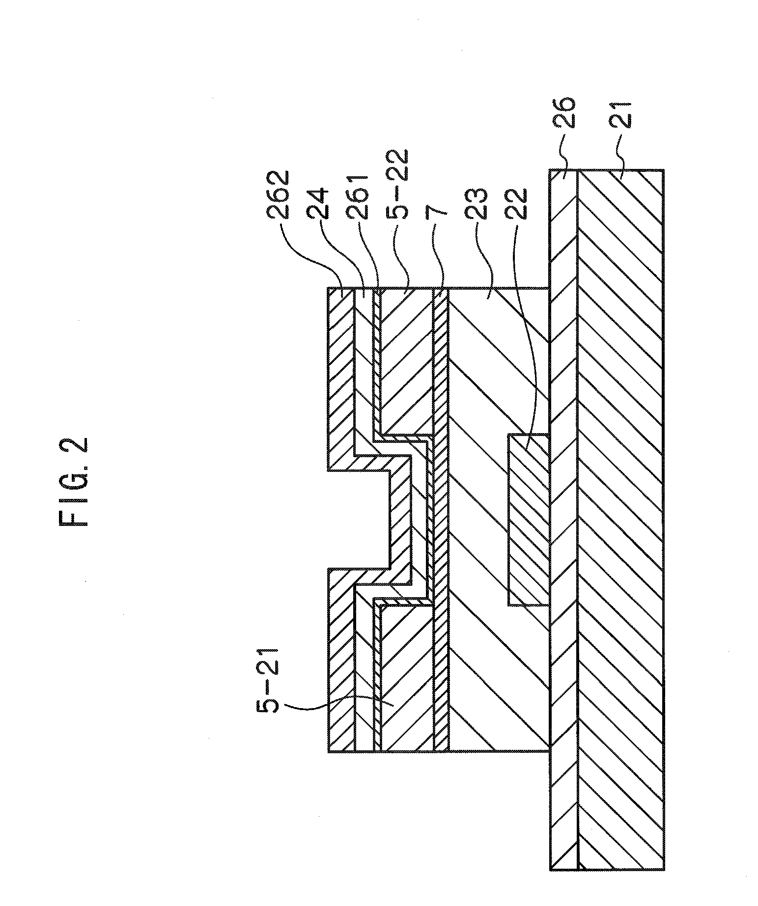
[0140]TFT element 1 of the invention having a configuration shown in FIG. 2 was fabricated as follows.
[0141]Substrate 21: a polyethylene naphthalate (PEN) film having a thickness of 125 μm was used.
[0142]Insulating layer 26: SiON was deposited to give a thickness of 500 nm by a sputtering deposition method.
[0143]Gate electrode 22: a molybdenum layer having a thickness of 40 nm was formed by a sputtering deposition method, which was subjected to photolithography and etching to form a stripe-shaped gate electrode.
[0144]Gate insulating layer 23: an acrylic resin was spin-coated, which was sintered to form a gate insulating layer 23 having a thickness of 0.5 μm.
[0145]Intermediate layer 7: on the gate insulating layer 23, an intermediate layer 7 having a thickness of 20 nm was provided by performing sputtering deposition of SiO2 through a metal mask at room temperature.
[0146]Source electrode 5-21 and drain electrode 5-22: on the whole surface ...
example 2
Fabrication of TFT Element 2 of the Invention
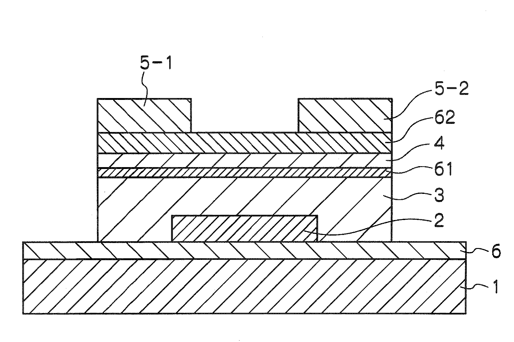
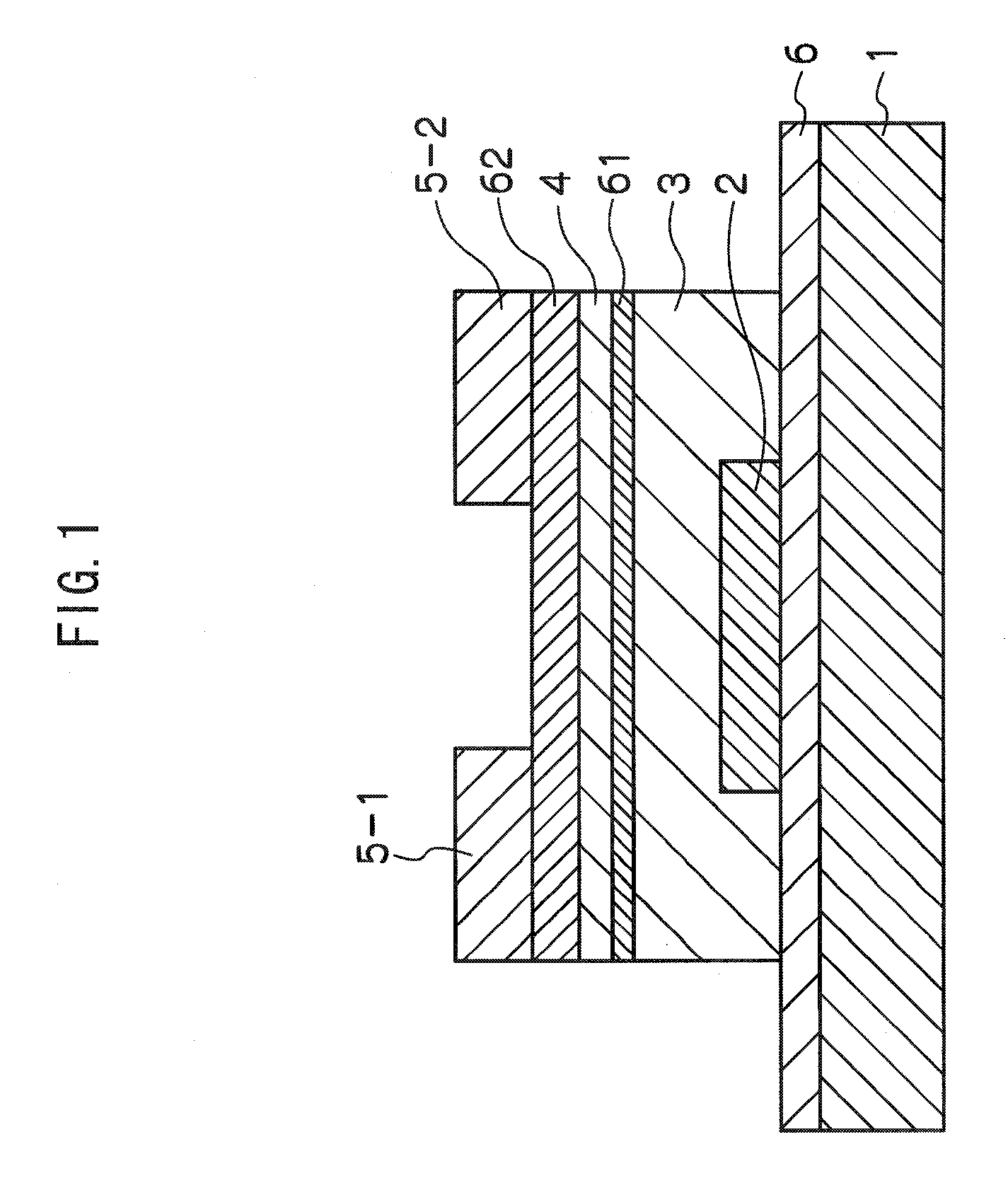
[0163]TFT element 2 of the invention having a configuration as shown in FIG. 1 was fabricated as follows.
[0164]Substrate 1: non-alkali glass having a thickness of 700 μm was used.
[0165]Gate electrode 2: a molybdenum layer having a thickness of 40 nm was formed by a sputtering deposition method, which was subjected to photolithography and etching to form a stripe-shaped gate electrode.
[0166]Gate insulating layer 3: SiO2 was formed by a sputtering deposition method at room temperature, thereby forming a gate insulating layer having a thickness of 200 nm.
[0167]First interface layer 61: on the gate insulating layer, a first interface layer having a thickness of 2.5 nm was provided by performing oxygen-introduced RF magnetron sputtering using a target having a composition of InGaZnO4 (hereinafter also referred to as “IGZO”) through a metal mask at room temperature to form an IGZO film.
[0168]Semiconductor layer (active layer) 4: on the first in...
example 3
Fabrication of TFT Element 3 of the Invention
[0171]In a similar manner to that in Example 2, a gate electrode, a gate insulating layer, and a first interface layer were successively formed on a non-alkali glass substrate.
[0172]First semiconductor layer: on the first interface layer, a first semiconductor layer having a thickness of 1.25 nm was provided by performing oxygen-introduced DC magnetron sputtering using a target having a composition of In3O2 including 10% by weight of ZnO (hereinafter also referred to as “IZO”) through a metal mask at room temperature to form an IZO film.
[0173]Intermediate interface layer: on the first semiconductor layer, an intermediate interface layer having a thickness of 2.5 nm was provided by performing oxygen-introduced RF magnetron sputtering using a target having a composition of IGZO through a metal mask at room temperature to form an IGZO film.
[0174]Second semiconductor layer: on the intermediate interface layer, a second semiconductor layer hav...
PUM
 Abstract
Description
Claims
Application Information
 - R&D
- Intellectual Property
- Life Sciences
- Materials
- Tech Scout
- Unparalleled Data Quality
- Higher Quality Content
- 60% Fewer Hallucinations
Browse by: Latest US Patents, China's latest patents, Technical Efficacy Thesaurus, Application Domain, Technology Topic, Popular Technical Reports.
© 2025 PatSnap. All rights reserved.Legal|Privacy policy|Modern Slavery Act Transparency Statement|Sitemap|About US| Contact US: help@patsnap.com


