
Layered ceramic electronic component and manufacturing method therefor

Inactive Publication Date: 2010-02-18
TDK CORPARATION
View PDF15 Cites 15 Cited by
  • Summary
  • Abstract
  • Description
  • Claims
  • Application Information

AI Technical Summary

Benefits of technology

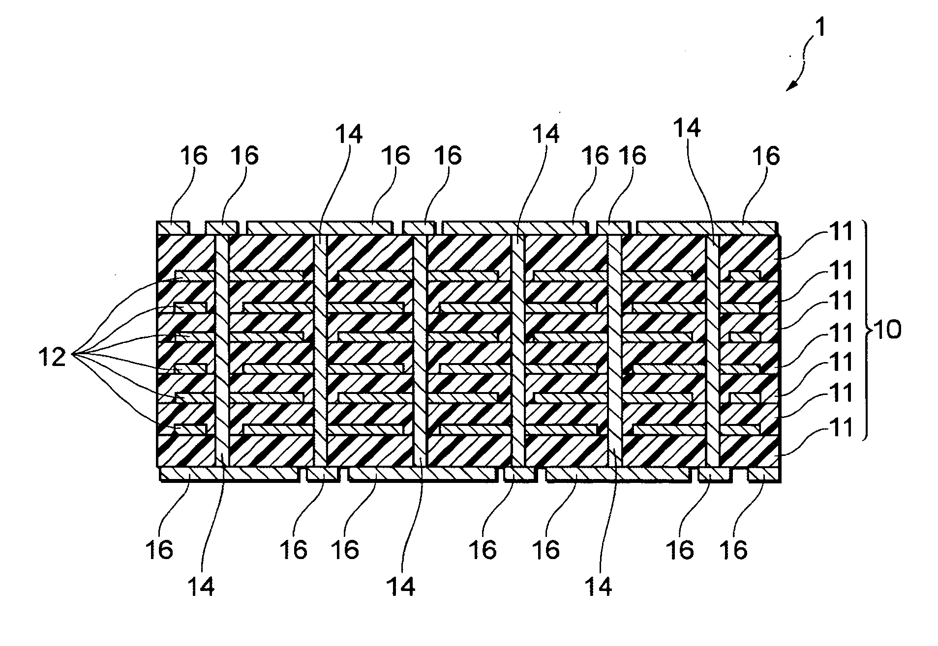
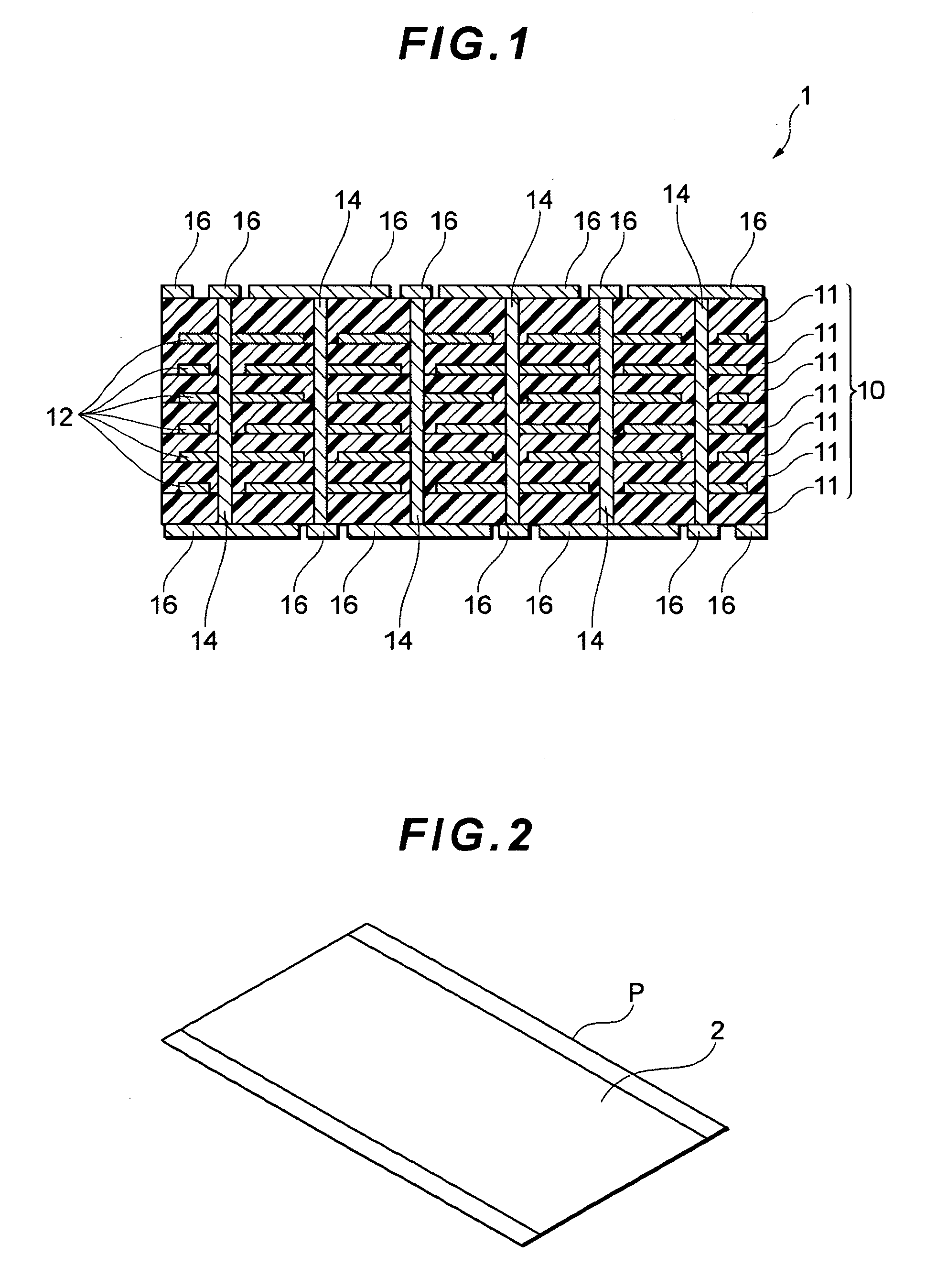
[0014]Next, a via-electrode forming conductive material is filled in the via hole of the resulting sintered body, followed by baking (in other words, firing again) to obtain a layered (multilayer) ceramic electronic component having a via electrode formed as a result of baking the conductive material in the via hole. Since the ceramic layer has already been fired into a sintered dielectric layer, it is possible to reduce the baking temperature to a sufficiently low level, that is, not greater than the melting point of the conductive material compared with the firing temperature of the ceramic layer and therefore suppress the expansion or contraction degree of the dielectric layer to a sufficiently low level. Accordingly, even if the via-electrode forming conductive material is baked under such a state, a decrease in a relative difference of expansion / contraction (expansion / contraction behavior) between the dielectric layers and the internal electrodes and via electrode can effectively prevent separation and formation of a gap between the dielectric layers and the internal electrodes and via electrode.
[0026]According to the layered (multilayer) ceramic electronic component and manufacturing method thereof of the present invention, the internal electrodes each contains the first metal having a melting point higher than the firing temperature of the ceramic material necessary for forming the dielectric layers; the via electrode contains the second metal having a melting point lower than the firing temperature of the ceramic material necessary for forming the dielectric layers and the third metal having a melting point higher than that of the second metal; and a content ratio of the third metal to the second metal is greater than 0 but less than 40 mass %. This enables to ensure reliable conduction between the internal electrodes and the via electrode and at the same time to effectively prevent occurrence of structural defects such as cracks in the dielectric layers.

Problems solved by technology

Detailed investigation of such production methods by the present inventors has however revealed that when a Cu-containing conductive material is used for the formation of a via electrode, the temperature (1100° C. or higher in the case of, for example, a BaTiO3 ceramic) required for firing the ceramic green sheet is higher than the melting point (1083° C.) of Cu so that Cu in the conductive material in the via hole melts during firing, leading to a failure in the formation of the via electrode.
It has also been confirmed that even if the via-electrode forming conductive material contains, in addition to Cu, another material such as Ni (melting point: 1453° C.) having a melting point higher than the firing temperature, melting of Ni is induced by melting of Cu, leading to a failure in the formation of a via electrode conductor.
At such a high temperature, however, since the ceramic green sheets and the conductive material layers differ in a thermal expansion coefficient, a difference caused by expansion or shrinkage during the firing procedure increases greatly and a gap tends to be created between dielectric layers and a via electrode which are formed by firing.
This makes it difficult to provide reliable conduction (electrical connection) between the via electrode and internal electrodes.
Moreover, the ceramic green sheets and the conductive material layers usually become relatively fragile as a result of removal of the binder at a relatively low temperature before firing.
Simultaneous firing with the conductive layers for forming the internal electrodes and the via electrodes at high temperatures under such a state increases a relative difference in elongation / shrinkage behavior between the ceramic green sheets and the conductive materials, which may lead to an inconvenience, that is, tendency to cause structural defects such as cracks in the dielectric layers and delamination between layers.
Generally speaking, as a result of detailed study on the above conventional multilayer ceramic electronic components, for example, multilayer ceramic capacitors, the present inventors have found that they may cause some inconveniences.
For example, sufficient conduction cannot always be provided between the internal electrodes and via electrode or cracks are liable to be formed in the dielectric layers.
The multilayer ceramic capacitor having such an inconvenience cannot exhibit its intended performances fully.

Method used


Image

  • Layered ceramic electronic component and manufacturing method therefor
  • Layered ceramic electronic component and manufacturing method therefor
  • Layered ceramic electronic component and manufacturing method therefor

Examples


examples

[0056]Examples of the present invention will hereinafter be described. It should however be borne in mind that the invention is not limited to or by these examples.

(Production of Layered (Multilayer) Ceramic Capacitor)

[0057]In a similar manner to the production procedures as described above, a layered (multilayer) ceramic capacitor having a similar structure to that illustrated in FIG. 1 was produced. The following are specific principal processing conditions. Described specifically, the thickness of a ceramic green sheet after drying was adjusted to approximately 5 μm. The thickness of a pattern of a conductive paste for internal electrode formation formed on the ceramic green sheet was adjusted to approximately 1.2 μm. A via hole formed in the stacked layers structure was made using a microdrill (drill diameter: 150 μm, rotation speed: 100000 rpm). Division into each separated piece was effected using a dicer having a cutting blade having a thickness of 0.35 mm. Removal of the bin...


PUM

PropertyMeasurementUnit
Percent by massaaaaaaaaaa

Abstract

Provided is a manufacturing method of a layered ceramic electronic component capable of preventing appearance of a gap between a dielectric layer and a via electrode to achieve reliable conduction between the via electrode and an internal electrode and at the same time, capable of effectively preventing occurrence of structural defects in the dielectric layer and the like.In a layered (multilayer) ceramic capacitor, dielectric layers and internal electrodes are stacked alternately. Of the internal electrodes, those placed opposite to each other via the dielectric layer are connected through the via electrode. The layered (multilayer) ceramic capacitor is produced by forming a via hole in stacked layers of a ceramic green sheet for forming the dielectric layer and a conductive paste for forming the internal electrode, followed by firing to obtain stacked layers having the dielectric layers and the internal electrodes formed therein. A conductive paste for forming the via electrode is filled in the via hole of the stacked layers and then baked to form the via electrode.

Description

BACKGROUND OF THE INVENTION[0001]1. Field of the Invention[0002]The present invention relates to a layered (multilayer) ceramic electronic component and a manufacturing method therefore (a method for producing the same).[0003]2. Description of the Related Art[0004]With a recent demand for further downsizing, thinning, and high-density packaging of electronic devices, there is also an eager demand for reducing the size or thickness of a circuit substrate to be used in electronic devices, which circuit substrate has thereon electronic components including active components, e.g., semiconductor devices such as IC chips and passive components, e.g., capacitors, inductors, thermistors, and resistors.[0005]Of these electronic components, particularly ceramic chip capacitors which are multilayer (layered, stacked) ceramic electronic components are strongly required to have a further increased capacity in addition to a reduced size or thickness. To satisfy the requirement for high-density p...

Claims


Application Information

Patent Timeline
IPC IPC(8): H05K1/09H05K1/11C03B29/00
CPCH01G4/232H01G4/2325H01G4/30H05K1/0306H05K2203/1438H05K3/4061H05K3/4611H05K3/4629H05K2201/0272H05K1/092H01L23/12
Inventor KOJIMA, TATSUYAHIROSE, OSAMU
Owner TDK CORPARATION
Learn More