
Three-terminal optical signal amplifying device

a technology of optical signal and amplifier, which is applied in the direction of semiconductor amplifier structure, semiconductor laser, instruments, etc., can solve the problems of large change in characteristics, large change in optical signal amplification, and high cost and complexity of optical circuitry system, so as to achieve sufficient optical signal amplification, sufficient intensity, and sufficient gain

Inactive Publication Date: 2009-11-12
MAEDA YOSHINOBU
View PDF18 Cites 0 Cited by
  • Summary
  • Abstract
  • Description
  • Claims
  • Application Information

AI Technical Summary

Benefits of technology

The device achieves stable and efficient optical signal amplification with reduced sensitivity to temperature changes and eliminates the need for multiple laser sources, simplifying the system and enhancing integration capabilities.

Problems solved by technology

Requiring a laser source in order to generate the second input light (bias light) at the second wavelength having the predetermined intensity that is input into the first semiconductor optical amplifying element together with the input light, causes the difficulty in integrating of the integrated circuit and small-sizing of the device.
Furthermore, requiring many laser sources upon using many three-terminal optical signal amplifying devices causes expensiveness and complexity in a system of optical circuitries.
Further, a change in the wavelength of the laser light causes such a disadvantage as an extensive change in its characteristics due to a change of the output from the first wavelength selecting element.

Method used


Image

  • Three-terminal optical signal amplifying device
  • Three-terminal optical signal amplifying device
  • Three-terminal optical signal amplifying device

Examples


Embodiment Construction

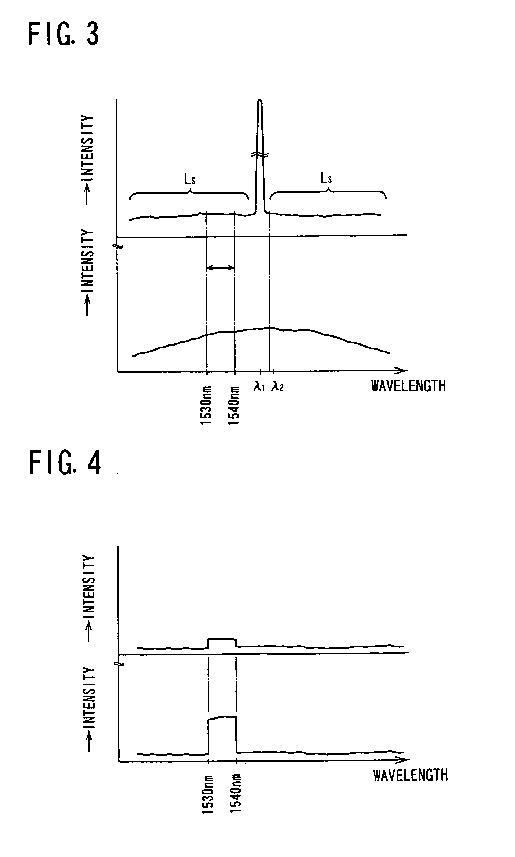
[0065]The semiconductor optical amplifying element is provided with the active layer constituted by the p-n junction to amplify the optical signal and is capable of generating the cross gain modulation. By the cross gain modulation an amplified laser light at the predetermined wavelength is output upon an input of a monochromatic laser light which is intensity-modulated, simultaneously, the neighboring light, that is, the spontaneous emission is output. The neighboring light has neighboring wavelengths around the wavelength of the input (or amplified) laser light, and the intensity of the neighboring light is increased or decreased in inverse proportion to the modulation of the input laser light in its intensity. Upon an input of a laser light having the predetermined intensity at the second wavelength which is within the range of the wavelengths of the spontaneous emission, the amplified laser light at the second wavelength is output which is modulated to be an inverse light with r...


PUM


Abstract

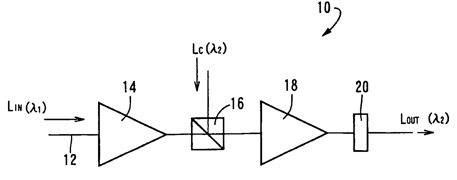
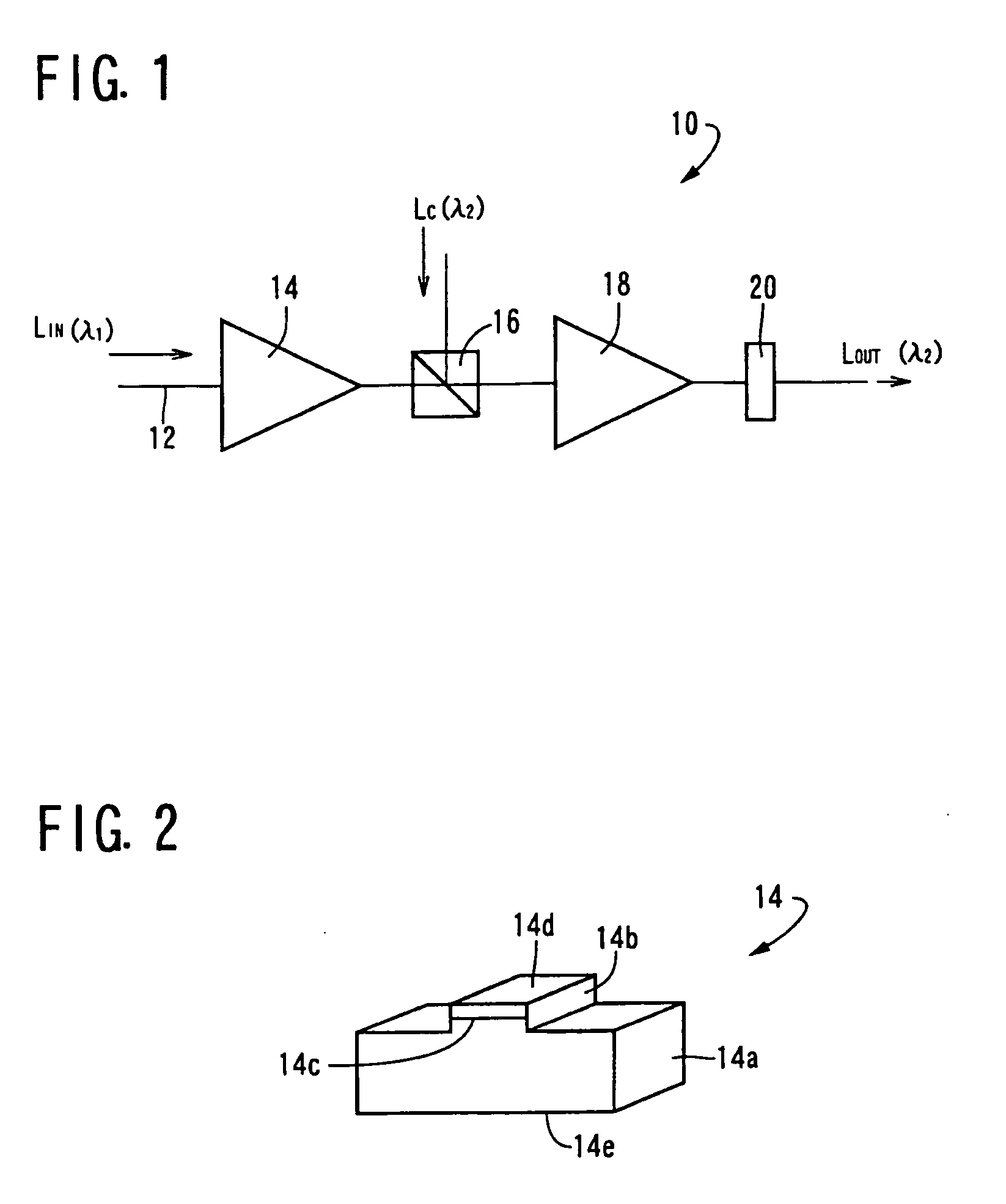
In the three-terminal optical signal amplifying device 10, a portion of the neighboring light LS at other wavelength than that of the first wavelength λ1 that is selected from the output light from the element 14 by the optical add drop filter 16, and the control light LC at the second wavelength λ2 input from the external are together input to the second semiconductor optical amplifying element 18. The output light including the output signal light LOUT at the second wavelength λ2 and the neighboring light at the neighboring wavelength to the second wavelength λ2 that is modulated and controlled by the control light LC in the cross gain modulation is output from the second semiconductor optical amplifying element 18. And the output signal light LOUT at the second wavelength λ2 passes through the wavelength selecting filter 20.

Description

[0001]This is a Division of application Ser. No. 11 / 632,718, which in turn is a National Stage of Application No. PCT / JP2005 / 003780, filed Mar. 4, 2005, which claims priority to Japanese Patent Application No. 2004-224726, filed Jul. 30, 2004. The disclosure of the prior applications are hereby incorporated by reference herein in their entirety.TECHNICAL FIELD[0002]The present invention relates to a three-terminal optical signal amplifying device suitable for optoelectronics such as optical communication, optical image processing, optical computation, optical measurement and optical integrated circuits, which are capable of advanced information processingBACKGROUND ART[0003]Actually, in optical communication, an optical signal that has been transmitted at a high speed is once converted into an electrical signal, which is subjected to data processing in an electronic circuitry, and the processed data signal is then reconverted into an optical signal to be transmitted. This incapabili...

Claims


Application Information

Patent Timeline
Patent Type & Authority Applications(United States)
IPC IPC(8): H01S3/00H01S5/00
CPCB82Y20/00G02F1/01708G02F1/3515G02F2/004G02F2201/30H04B10/2914H01S5/005H01S5/026H01S5/1003H01S5/50H01S5/5072G02F2203/70
Inventor MAEDA, YOSHINOBU
Owner MAEDA YOSHINOBU
Learn More