
Silicon substrate for magnetic recording and method for manufacturing the same

Inactive Publication Date: 2009-09-10
SHIN ETSU CHEM IND CO LTD
View PDF0 Cites 3 Cited by
  • Summary
  • Abstract
  • Description
  • Claims
  • Application Information

AI Technical Summary

Benefits of technology

[0024]The single crystalline Si substrate has been widely used as a substrate for manufacturing an LSI. Since the single crystalline Si substrate excels in surface flatness, environmental stability, and reliability, as well as high rigidity compared with the rigidity of glass, the single crystalline Si substrate is suitable for an HDD substrate. In addition, the single crystalline Si substrate shows semiconductive behavior unlike an insulating glass substrate, often contains p-type or n-type dopant, and has conductivity to a certain degree. Therefore, “charge-up” is relatively reduced in the sputtering process, enabling the direct sputtering or the bias sputtering of a metal film. Furthermore, since the single crystalline Si substrate has favorable heat conductivity and high heat resistance, the substrate can easily be heated to a high temperature, and good compatibility with the sputtering film forming is extremely high. Moreover, since the crystal purity of the Si substrate is extremely high, there are advantages that the surface of the substrate after processing is stable, and the temporal change can be ignored.
[0025]However, the only weak point is the high costs of the 48 mm-diameter or larger single crystalline Si wafer.
[0026]The present inventors have also proposed the use of a polycrystalline silicon (Si) substrate as a substrate of a HDD recording film. Polycrystalline Si has various selections of material in terms of purity, and excels in the cost performance of the substrate.
[0027]The use of a polycrystalline substrate as it is, and the use of a polycrystalline substrate after forming an oxide film on the surface and planarizing and flattening the film have been developed. Although the former has a simple configuration wherein the single crystalline Si is simply replaced by the polycrystalline Si, the polycrystalline Si substrate is relatively inferior to the single crystalline Si substrate in the strength of the substrate and the defect of polished surface. The strength of the latter is higher than the strength of the single crystalline Si substrate, and since the silicon oxide film is amorphous, excellent surface characteristics can be obtained after polishing. However, since the oxide film having low thermal conductivity is present on the surface, the heat conductivity from the surface of the substrate in the vertical direction is affected. Particularly in the heat-assisted magnetic recording, the design for releasing heat applied in writing may be affected.
[0028]The present invention has been made in view of the above problems, and an object of the present invention is to provide a surface-coated polycrystalline Si substrate for a magnetic recording medium and a recording medium, which are aimed at substrates for magnetic recording having a diameter of 48 mm or more, the polycrystalline Si substrate having excellent surface flatness and smoothness as well as high cost-effectiveness without impairing most thermal conductive properties of the polycrystalline Si substrate.
[0034]A polycrystalline Si substrate for a magnetic recording medium, which have excellent surface flatness and smoothness as well as high cost-effectiveness, and a recording medium can be provided without impairing a good thermal conductive property of a polycrystalline Si substrate by polishing the silicide film or the alloy film.

Problems solved by technology

However, the only weak point is the high costs of the 48 mm-diameter or larger single crystalline Si wafer.

Method used


Image

  • Silicon substrate for magnetic recording and method for manufacturing the same
  • Silicon substrate for magnetic recording and method for manufacturing the same
  • Silicon substrate for magnetic recording and method for manufacturing the same

Examples


examples

[0065]The present invention will be more specifically described below by way of Examples, but the present invention is not intended to be limited to these Examples.

[0066]A polycrystalline Si wafer (156 mm square, and 0.6 mm thickness) having a purity of “5 nines” was prepared (S1). Four substrates per wafer was obtained by coring Si substrates, each having outside diameter 65 mm and inside diameter 20 mm, from this polycrystalline Si wafer with a laser processing machine (YAG laser, wavelength 1064 nm) (S2). These substrates were subjected to inner and outer coring (S3), adjusting thickness processing (S4), and circumferential surface polishing (S5). Then, a major surface of the polycrystalline Si substrate was subjected to a rough polishing (S6). The rough polishing was performed, using a double-side polishing machine, with slurry of colloidal silica (an average grain diameter 40 nm) of pH 8.5, at a polishing pressure of 10 kg / cm2, for 10 minutes to 30 minutes, and at the maximum 1...


PUM


Abstract

A Si substrate for a magnetic recording medium having excellent surface flatness without making a processing process and deposition process of a magnetic recording layer complex, as well as a thermal conductivity that is unchanged from a bulk substrate of a single crystal and a polycrystal is provided. A metal film is deposited (S7) on a polycrystalline silicon substrate after rough polishing (S6) and silicidated or silicon-alloyed (S8). Thereafter, the film is subjected to precision polishing (S9) such as CMP polishing to increase the flatness of the substrate. Accordingly, the Si substrate for a magnetic recording medium can obtain a flat and smooth surface without being influenced by a difference between crystal orientations of the polycrystalline grains and the presence of crystal grain boundary, and can obtain heat resistance and a thermal conductivity approximately equivalent to a bulk Si substrate.

Description

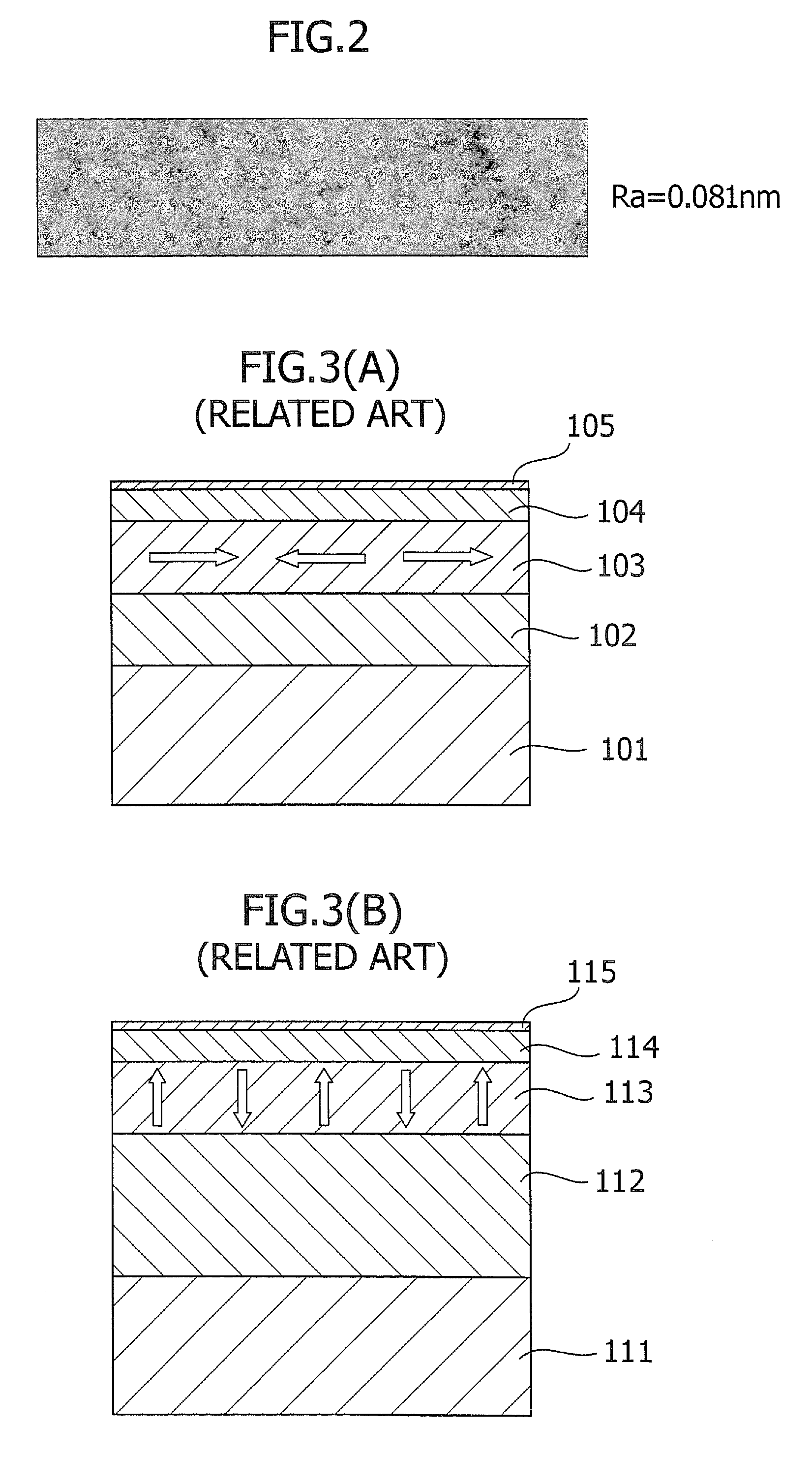
CROSS-RELATED APPLICATIONS[0001]This application claims priority from Japanese Patent Application No. 2008-057785; filed Mar. 7, 2008, the disclosure of which is incorporated herein by reference in its entirety.BACKGROUND OF THE INVENTION[0002]1. Field of the Invention[0003]The present invention relates to a polycrystalline silicon substrate used for magnetic recording, and a method for manufacturing the same.[0004]2. Description of the Related Art[0005]In the technical field of magnetic recording, a hard disk device has been essential as a primary external recording device suitable for electronic devices such as personal computers. A hard disk is incorporated into the hard disk device as a magnetic recording medium, and conventional hard disks have adopted a system known as the “in-plane magnetic recording system (horizontal magnetic recording system)” in which magnetic information is written horizontally on the disk surface.[0006]FIG. 3(A) is a schematic sectional view for illustr...

Claims


Application Information

Patent Timeline
IPC IPC(8): B32B3/00B32B5/00B05D5/12
CPCG11B5/7315Y10T428/24355Y10T428/265G11B5/8404G11B5/73915
Inventor OHASHI, KEN
Owner SHIN ETSU CHEM IND CO LTD
Learn More