
Panel-type input device, method of manufacturing panel-type input device, and electronic apparatus having panel-type input device

a technology of input device and input device, which is applied in the manufacture of contact members, conductive layers on insulating supports, instruments, etc., can solve the problems of raising the manufacturing cost of the input device and achieve the effect of increasing the surface resistivity

Active Publication Date: 2009-08-13
FUJITSU LTD
View PDF9 Cites 62 Cited by
  • Summary
  • Abstract
  • Description
  • Claims
  • Application Information

AI Technical Summary

Benefits of technology

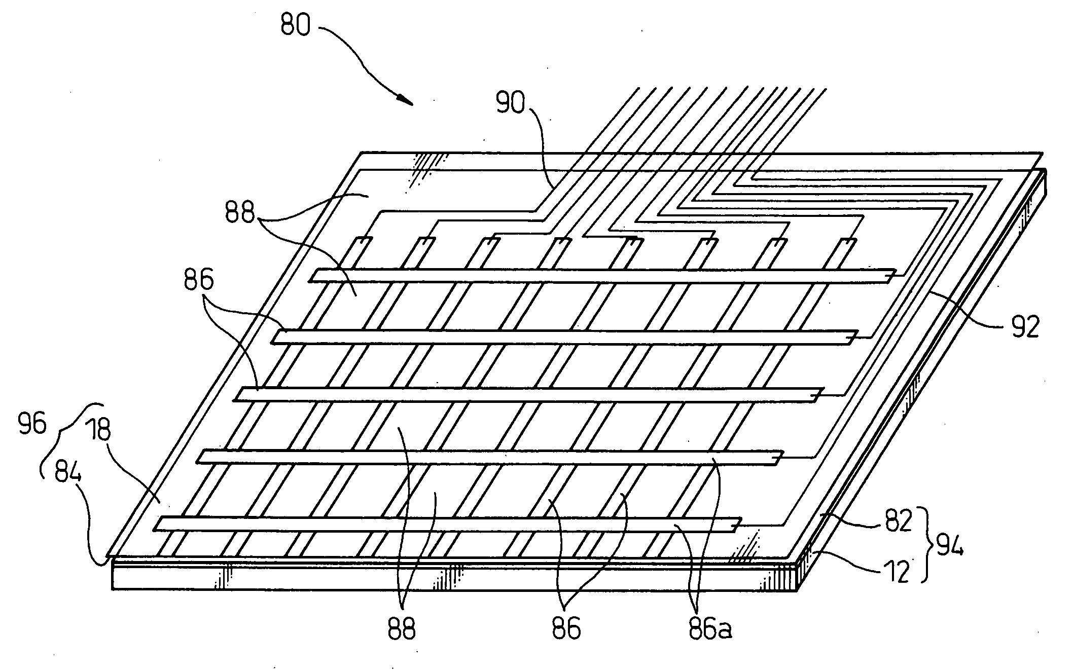
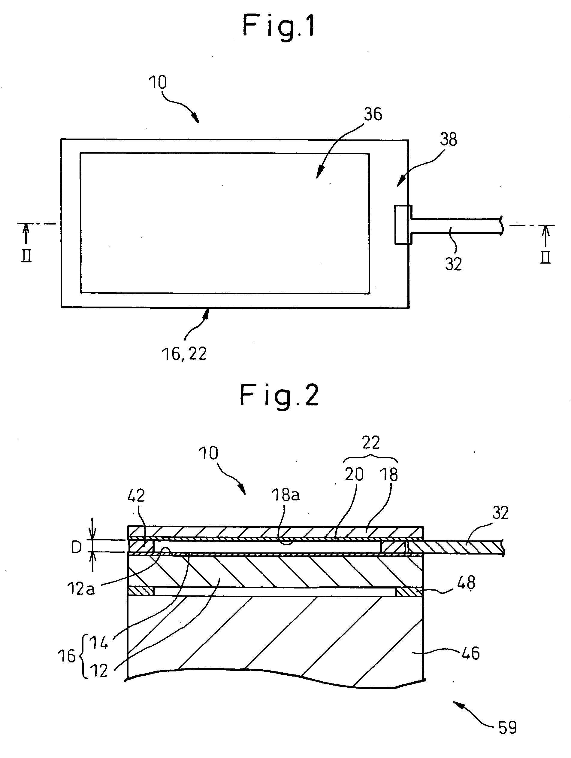
[0014]It is an object of the present invention to provide a panel-type input device equipped with a conducting polymer used as a conductive coat, which can reduce a panel thickness and can form an insulating region at a desired position with a desired pattern at low cost.
[0015]It is another object of the present invention to provide a method of manufacturing a panel-type input device equipped with a conducting polymer used as a conductive coat, which can reduce a panel thickness and can form an insulating region at a desired position with a desired pattern at low cost.
[0016]It is still another object of the present invention to provide an electronic apparatus including a panel-type input device equipped with a conducting polymer used as a conductive coat, which can reduce a panel thickness and can form an insulating region at a desired position with a desired pattern at low cost.
[0017]It is a still further object of the present invention to provide a panel-type input device configured as a touch panel and a method of manufacturing the panel-type input device, which can eliminate drawbacks, such that a boundary line between a detecting area and an inoperative area may be visible or a detecting area and an inoperative area may be visually distinguishable, and thus can improve the visibility of a display screen through the panel-type input device.

Problems solved by technology

On the other hand, the process for forming the insulating region by locally removing the conductive coat through etching or the like requires the provision of a coating removing apparatus such as etching equipment and the increased number of processing steps, which may raise the manufacturing cost of the panel-type input device.

Method used


Image

  • Panel-type input device, method of manufacturing panel-type input device, and electronic apparatus having panel-type input device
  • Panel-type input device, method of manufacturing panel-type input device, and electronic apparatus having panel-type input device
  • Panel-type input device, method of manufacturing panel-type input device, and electronic apparatus having panel-type input device

Examples


experiment 1

[Experiment 1]

[0087]As a sample of the electrode plate 16, 22 of the panel-type input device 10, an electrode plate (50 mm×60 mm) having a configuration in which a conductive coat (100 nm in thickness) formed from polythiophene-based conducting polymer (PEDOT / PSS) was coated onto a substrate (188 μm in thickness) formed from a PET film was prepared. The initial surface resistivity (pursuant to, e.g., JIS K6911) of the conductive coat of this electrode plate was 653Ω / □ (ohm / square). Then, the electrode plate was irradiated with ultraviolet light with 365 nm peak-wavelength including 245 nm wavelength and 1000 mW / cm2 irradiance, from a high-pressure mercury lamp, in the atmosphere containing 0.1 ppm-100 ppm ozone, in a direction vertical to the surface of the conductive coat, at a scan speed of 0.67 m / min, by using an ultraviolet light irradiator UVC-02516 (manufactured by USHIO Inc., Tokyo, Japan). The irradiance light quantity of ultraviolet light irradiated in a single scan (referr...

experiment 2

[Experiment 2]

[0089]In relation to the aforementioned sample of the electrode plate, a conductivity controlling agent selected from a group including an oxidizing reagent such as hypochlorous acid, chloric acid, nitric acid, nitrous acid, sulfuric acid, sulfurous acid, etc., and a basic reagent such as sodium hydroxide, potassium, ammonium, tetraethylammonium hydroxide, etc., was contacted with the conductive coat through the mask 56 (FIG. 5), so as to increase the surface resistivity of the desired region of the conductive coat. As a result, two regions having mutually different surface resistivity were successfully formed in the conductive coat, which can be used as the conductive coats 14, 20 of the electrode plates 16, 22 of the panel-type input device 10. In particular, a basic reagent containing 10% sodium hydroxide solution as a major component was excellent in a resistivity increasing function, and the surface resistivity of the desired region of the conductive coat was nece...

experiment 3

[Experiment 3]

[0090]The aforementioned sample of the electrode plate was prepared by modifying the conductive coat so as to be formed from polythiophene-based conducting polymer (PEDOT / PSS) containing 3% benzoyl peroxide. The initial surface resistivity (pursuant to, e.g., JIS K6911) of the conductive coat of this electrode plate was 698Ω / □ (ohm / square). Then, the electrode plate was irradiated with ultraviolet light with 365 nm peak wavelength and 1000 mW / cm2 irradiance, from a high-pressure mercury lamp, in a direction vertical to the surface of the conductive coat, at a scan speed of 5 m / min, by using the same apparatus as in Experiment 1. The irradiance light quantity of ultraviolet light in a single scan (referred to as a unit light quantity) was 500 mJ / cm2. FIG. 15 shows a mode of change in the surface resistivity of the conductive coat, measured through the repeated irradiation of the unit light quantity. As shown in FIG. 15, it has been proved that the surface resistivity of...


PUM

PropertyMeasurementUnit
Thicknessaaaaaaaaaa
thicknessaaaaaaaaaa
thicknessaaaaaaaaaa

Abstract

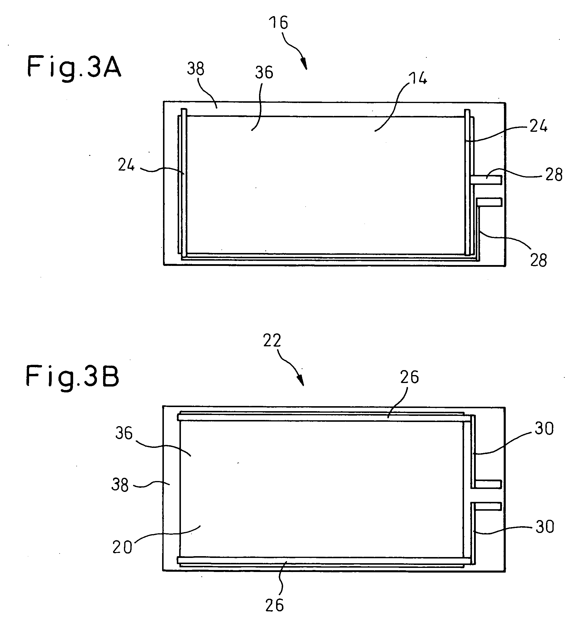
A panel-type input device including a pair of electrode plates, each electrode plate having a substrate and a conductive coat provided on a surface of the substrate, the conductive coat of each electrode plate being formed from a conducting polymer. The conductive coat of each electrode plate includes a detecting area adapted to detect a touch input and an inoperative area disposed adjacent to the detecting area, the inoperative area having a surface resistivity higher than a surface resistivity of the detecting area. A parallel electrode pair adapted to apply a voltage to the conductive coat is formed in the detecting area, and conductors connected to the parallel electrode pair are formed in the inoperative area. The inoperative area insulates the conductors from the detecting area.

Description

BACKGROUND OF THE INVENTION[0001]1. Field of the Invention[0002]The present invention relates to a panel-type input device. The present invention also relates to a method of manufacturing a panel-type input device. The present invention further relates to an electronic apparatus having a panel-type input device.[0003]2. Description of the Related Art[0004]A panel-type input device has been known as an input device (or a coordinates detecting device) of an electronic apparatus including a display unit, such as a personal computer, a personal digital assistant (PDA), an automatic teller machine (ATM), etc., which is operated to indicate two-dimensional coordinate data in the display unit by an operator touching a desired point on a panel surface with his or her finger or with a pen. In particular, a panel-type input device with a transparent structure which can be mounted on a screen of a display unit, such as a liquid crystal display (LCD), a plasma display panel (PDP), a cathode ray...

Claims


Application Information

Patent Timeline
Patent Type & Authority Applications(United States)
IPC IPC(8): G06F3/045H01R43/00
CPCG06F3/045H01L2924/0002Y10T29/49117G01N27/22G06F3/044Y10T29/49204H01L2924/00G06F3/0445G06F3/0446G06F3/047G06F2203/04103H01B5/14
Inventor ENDO, MICHIKOIWATA, HIDEKITAKEI, FUMIOKASHIKAWA, TAKAHIRO
Owner FUJITSU LTD
Learn More