
Non-volatile memory device and method of manufacturing the same

a technology of non-volatile memory and manufacturing method, which is applied in the direction of digital storage, semiconductor devices, instruments, etc., can solve the problems of difficult to prevent erroneous reading and variation of off leakage properties, so as to reduce the variation improve the yield of phase change memory, and reduce the effect of the electric property of the diod

Inactive Publication Date: 2009-07-30
HITACHI LTD
View PDF5 Cites 19 Cited by
  • Summary
  • Abstract
  • Description
  • Claims
  • Application Information

AI Technical Summary

Benefits of technology

[0009]The present invention intends to provide a phase change memory at high yield with less variation in the electric property of a diode which is the selection device by eliminating crystal grain boundaries in polysilicon during a manufacturing process.
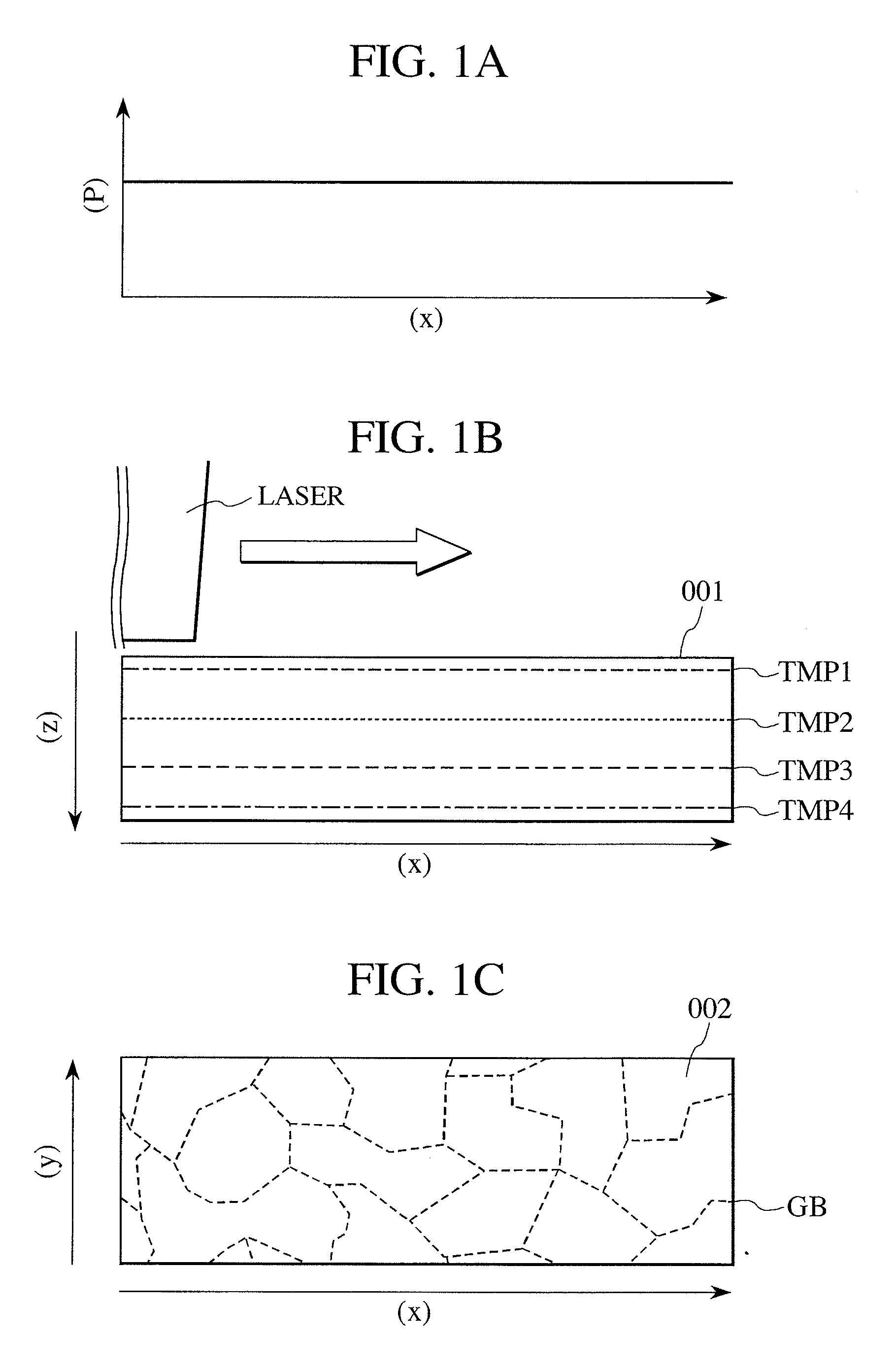
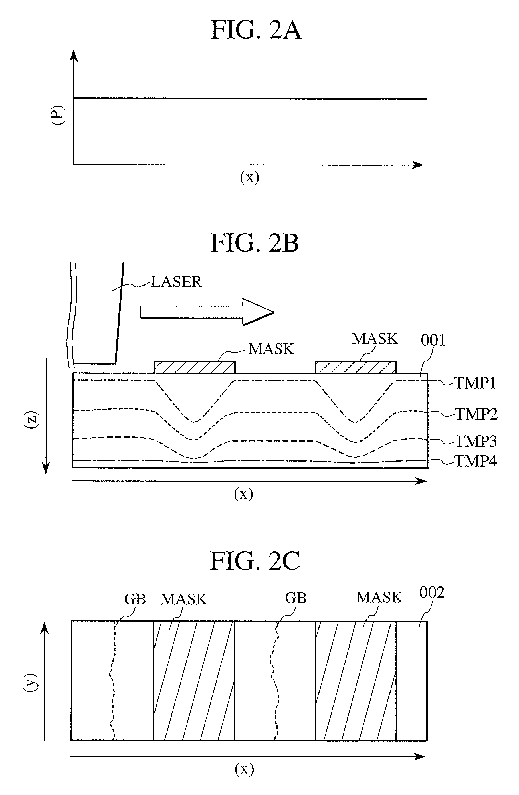
[0011]In a first method of the invention, the laser power is constant as shown in FIG. 2A. When a light reflection layer MASK is provided above the amorphous silicon layer 001 which is the specimen as shown in FIG. 2B, the laser is absorbed to or reflected at the light reflection layer MASK, thereby providing a temperature profile which differs depending on the position (x) in the specimen. Since the temperature below the light reflection layer MASK is lowered and the portion is cooled precedingly, crystallization occurs from the portion below the light reflection layer MASK. As a result, when viewing the specimen from above the upper surface, crystal grain boundaries GB of the obtained polysilicon can be controlled so that they are generated on the outside of the light reflection layer MASK as shown in FIG. 2C. As will be described later specifically for an embodiment to be described later, since a diode which is a selection device is formed at a portion below the light reflection layer MASK, variation of the electric property of the diode is decreased and the yield of the phase change memory can be improved.
[0012]Further, in a second method of the invention, as shown in FIG. 3A, the laser power is modulated relatively lower in a region PTN where a selection device is formed, thereby providing a temperature profile which is different depending on the position (x) in the specimen as shown in FIG. 3B. Since the temperature below the region PIN where a selection device is formed is lowered and the portion is cooled precedingly, crystallization occurs from the portion below the region PIN. As a result, when viewing the specimen from above the upper surface, crystal grain boundaries GB of the obtained polysilicon layer 002 can be controlled such that they are generated on the outside of the region PTN in which the selection device is formed as shown in FIG. 3C. Like the first method that has been explained with reference to FIG. 2A to FIG. 2C, variation of the electric property of the diode is decreased and the yield of the phase change memory can be improved. In the second method, since it is not necessary to additionally provide a light reflection layer, the number of manufacturing steps is not increased.
[0013]According to the invention, since a memory matrix can be constituted while avoiding the effect of the crystal grain boundaries in the diode layer, a non-volatile memory can be manufactured at a good yield.

Problems solved by technology

However, in a diode using polysilicon, since a number of crystal grain boundaries are present in a film, the off leak property varies greatly and it is difficult to prevent erroneous reading.

Method used


Image

  • Non-volatile memory device and method of manufacturing the same
  • Non-volatile memory device and method of manufacturing the same
  • Non-volatile memory device and method of manufacturing the same

Examples


embodiment 1

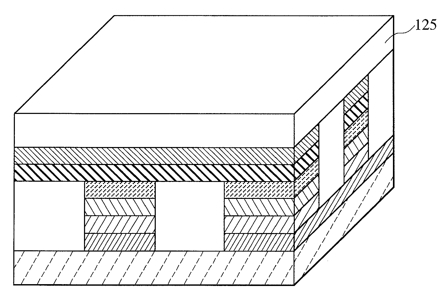
[0055]In this embodiment, a semiconductor device of the invention is formed above a semiconductor substrate 101 shown in FIG. 5. The semiconductor substrate 101 has a peripheral circuit portion 004 for operating a memory matrix of a non-volatile memory. The peripheral circuit is manufactured by using an existent CMOS technique. FIG. 4A to FIG. 4C show a positional relationship between a memory matrix portion 005 and the peripheral circuit portion 004 in the cross section of the semiconductor substrate (silicon substrate). In this embodiment, description is to be made with an example of manufacturing the memory matrix portion 005 above the peripheral circuit portion 004 as shown in FIG. 4A, but the positional relation between the memory matrix portion 005 and the peripheral circuit portion 004 may be such that the memory matrix portion 005 and the peripheral circuit portion 004 are in an identical layer as shown in FIG. 4B, or the memory matrix portion 005 and the peripheral circuit ...

embodiment 2

[0078]In this embodiment, a memory cell of the invention is formed above a semiconductor substrate 101 shown in FIG. 19. The semiconductor substrate 101 includes a peripheral circuit for operating the memory matrix of a non-volatile memory. The peripheral circuit is manufactured by an existent CMOS technique. The positional relation between the peripheral circuit and the memory matrix is identical with that in Embodiment 1.

[0079]FIG. 19 shows the structure of depositing, above the semiconductor substrate 101, a first metal interconnect layer 102, a first amorphous silicon layer 103, and a second amorphous silicon layer 104 successively. The first metal interconnect layer 102 is formed by sputtering. The material of the first metal interconnect layer 102 is tungsten. Since a material of lower resistivity shows less voltage drop and can provide a read current, aluminum or copper which is a material of lower resistivity than that of tungsten is more preferred. Further, a metal compound...

embodiment 3

[0093]In this embodiment, a memory cell of the invention is formed above a semiconductor substrate 101 shown in FIG. 27. The semiconductor substrate 101 includes a peripheral circuit for operating the memory matrix of a non-volatile memory. The peripheral circuit is manufactured by using an existent CMOS technique. The positional relation between the peripheral circuit and the memory matrix is identical with that in Embodiment 1. A great difference between this embodiment and Embodiments 1 and 2 is that the diode layer is on the non-volatile recording material layer.

[0094]FIG. 27 shows the structure of depositing, above the semiconductor substrate 101, the first metal interconnect layer 102, the non-volatile recording material layer 115, the buffer layer 134, the first amorphous silicon layer 103, the second amorphous silicon layer 104 and the light reflection layer 107 successively. The first metal interconnect layer 102 is formed by sputtering. The material of the first metal inte...


PUM

PropertyMeasurementUnit
thicknessaaaaaaaaaa
thicknessaaaaaaaaaa
thicknessaaaaaaaaaa

Abstract

In a phase change memory, electric property of a diode used as a selection device is extremely important. However, since crystal grain boundaries are present in the film of a diode using polysilicon, it involves a problem that the off leak property varies greatly making it difficult to prevent erroneous reading. For overcoming the problem, the present invention provides a method of controlling the temperature profile of an amorphous silicon in the laser annealing for crystallizing and activating the amorphous silicon thereby controlling the crystal grain boundaries. According to the invention, variation in the electric property of the diode can be decreased and the yield of the phase-change memory can be improved.

Description

CLAIM OF PRIORITY[0001]The present application claims priority from Japanese patent application JP 2008-017013 filed on Jan. 29, 2008, the content of which is hereby incorporated by reference into this application.BACKGROUND OF THE INVENTION[0002]1. Field of the Invention[0003]The present invention relates to a method of manufacturing an electrically rewritable phase change memory device for non-volatile memory storage of a resistance value determined by the phase change of a metal compound between a crystalline state and an amorphous state.[0004]2. Description of the Related Arts[0005]Non-volatile memory devices include those using a crystalline state and an amorphous state of a metal compound as memory information. As the memory material, tellurium compounds are generally used. The principle of storing information due to the difference of the reflectance thereof has been used generally in optical information memory media such as DVD (Digital Versatile Disk).[0006]In recent years, ...

Claims


Application Information

Patent Timeline
Patent Type & Authority Applications(United States)
IPC IPC(8): H01L47/00H10B69/00
CPCG11C11/5678G11C13/0004G11C2213/71G11C2213/72H01L21/8221H01L27/101H01L27/1285H01L27/2481H01L45/06H01L45/1233H01L45/144H01L45/1675H01L27/2409H10B63/20H10B63/84H10N70/231H10N70/826H10N70/8828H10N70/063H10N70/8825
Inventor KINOSHITA, MASAHARUTERAO, MOTOYASUMATSUOKA, HIDEYUKISASAGO, YOSHITAKAKIMURA, YOSHINOBUSHIMA, AKIOTAI, MITSUHARUTAKAURA, NORIKATSU
Owner HITACHI LTD
Learn More