Manufacturing method of low-k thin films and low-k thin films manufactured therefrom

Inactive Publication Date: 2009-07-23
RES & BUSINESS FOUNDATION SUNGKYUNKWAN UNIV
View PDF7 Cites 3 Cited by
  • Summary
  • Abstract
  • Description
  • Claims
  • Application Information

AI Technical Summary

Benefits of technology

[0009]In order to find solutions for the above-mentioned problems, the present inventors had researched a method for manufacturing low-k thin film, wherein the dielectric constant (k) is greatly lower than the prior art. As a result, they have found in the present invention that a plasma-polymerized polymeric thin film deposited by the PECVD process using cyclic-shaped precursors can form pores not exceeding the size of several nm, and shorten the complicated process and the period of time for pre- and post-treatments in the spin casting process, and also that a novel method can improve a dielectric constant and mechanical properties (e.g., hardness and elastic modulus) of a material by using, for example, post-heat treatments.

Problems solved by technology

High temperature at which a predetermined thermal CVD process performs can cause damages to the structure of the device which has a film formed on the surface of the substrate.
Silicon dioxide (SiO2) or silicon oxyfluoride (SiOF), which have been mainly used as interlayer dielectric till lately, have the problems of high capacitance, long RC delay, etc., when manufacturing ultra large-scale integrated circuits of no more than 0.5 μm.
However, no concrete solution has been proposed.
However, they are unsuitable for the applications since the upper limit of heat-resisting is lower than 450° C. so that the thermal stability is poor, and also, they have various difficulties in manufacturing devices since the size of pores is so large that the pores are not uniformly distributed in the film.
Additionally, they have other problems, including bad adhesion with wiring materials of upper and lower sides, generation of high stress by the organic polymeric thin film-specific thermal curing, and depreciated reliability of the device by alteration of dielectric constant (k) because of adsorption of surrounding water.

Method used


Image

  • Manufacturing method of low-k thin films and low-k thin films manufactured therefrom
  • Manufacturing method of low-k thin films and low-k thin films manufactured therefrom
  • Manufacturing method of low-k thin films and low-k thin films manufactured therefrom

Examples


Embodiment Construction

[0029]The description that follows describes, illustrates and exemplifies one or more particular embodiments of the present invention in accordance with its principles. This description is not provided to limit the invention to the embodiments described herein, but rather to explain and teach the principles of the invention in such a way to enable one of ordinary skill in the art to understand these principles and, with that understanding, be able to apply them to practice not only the embodiments described herein, but also other embodiments that may come to mind in accordance with these principles. The scope of the present invention is intended to cover all such embodiments that may fall within the scope of the appended claims, either literally or under the doctrine of equivalents.

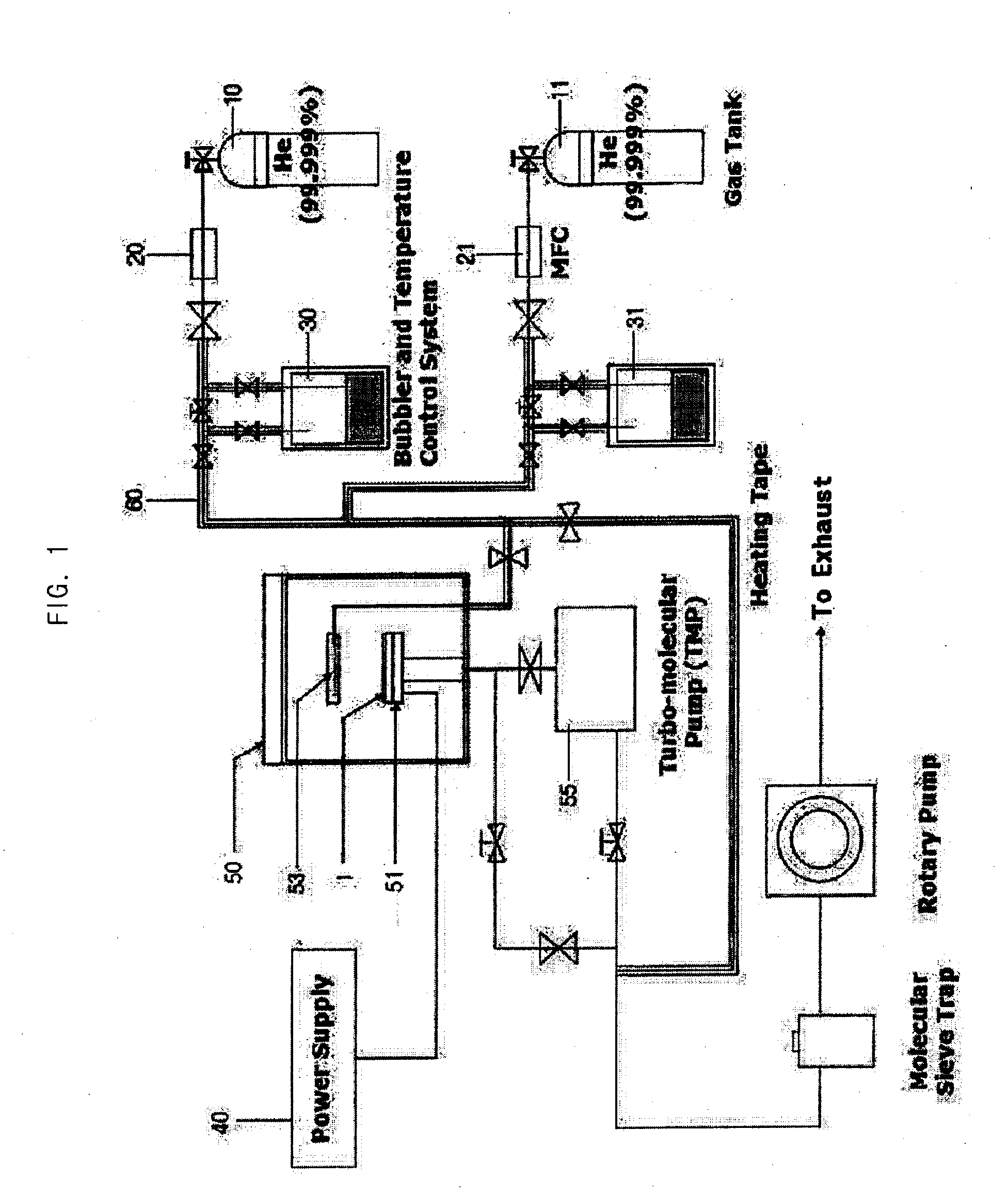
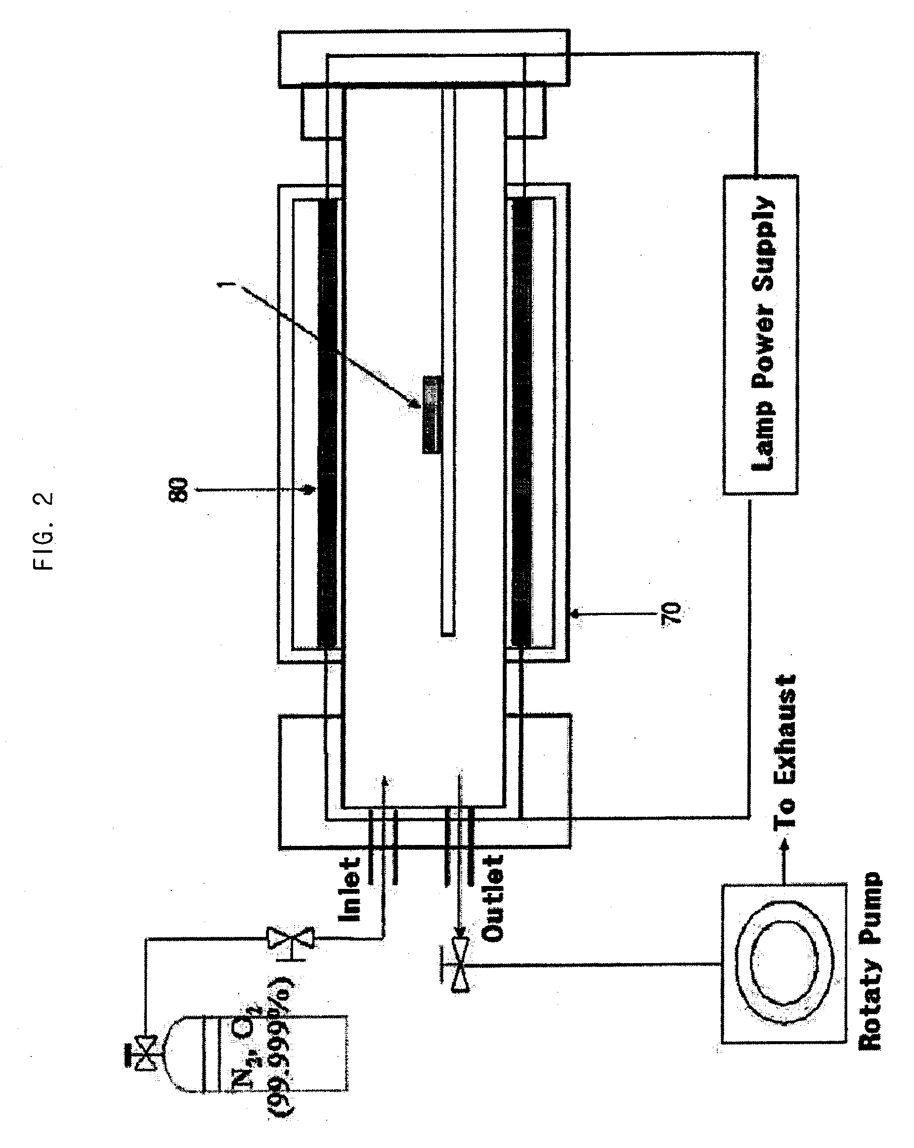
[0030]The method of manufacturing a low-k thin film for semiconductor devices according to an embodiment of the present invention is disclosed in detail below, together with the attached drawings, so that...


PUM

PropertyMeasurementUnit
Temperatureaaaaaaaaaa

Abstract

The present invention relates to a method of manufacturing a low-k thin film and the low-k thin film manufactured therefrom. More specifically, the method of manufacturing a low-k thin film in accordance with an embodiment of the present invention includes subjecting thin film, which is formed by plasma polymerization, to post-heat treatment using an RTA device, and low-k thin film manufactured therefrom.A method of manufacturing a low-k thin film in accordance with an embodiment of the present invention includes: evaporating a precursor solution including decamethylcyclopentasiloxane and cyclohexane in a bubbler; inflowing the evaporated precursor from the bubbler to a plasma deposition reactor; depositing a plasma-polymerized thin film on a substrate in the reactor by using a plasma in the reactor; and post-heat-treating by an RTA device.

Description

CROSS REFERENCE TO RELATED APPLICATION[0001]The present Non-Provisional Patent Application is a national stage continuation application of International Application No. PCT / KR2007 / 003107, filed on 27 Jun. 2008, which claims priority to Korean Patent Application No. 10-2007-0029594, filed on 27 Mar. 2008, both of which are incorporated herein by reference.TECHNICAL FIELD[0002]The present invention relates to a method of manufacturing a low-k thin film and the low-k thin film manufactured therefrom. More specifically, the present invention relates to a low-k thin film manufacturing method comprising subjecting a thin film which is formed by plasma polymerization to post-heat treatment using an RTA device, and the low-k thin film manufactured therefrom.BACKGROUND OF THE INVENTION[0003]These days, one of the major steps in manufacturing semiconductor devices involves forming metal and dielectric thin films on a substrate by a gaseous chemical reaction. The said thin film deposition proc...

Claims


Application Information

Patent Timeline
IPC IPC(8): C08L83/04C23C16/513
CPCB05D1/62B05D3/0254H01L21/02126H01L21/3122H01L21/02216H01L21/02274H01L21/02337H01L21/02203H01L21/205C23C16/448C23C16/56C23C16/505C23C16/401H01L21/67207H01L21/68714
Inventor JUNG, DONG-GEUNYANG, JAE-YOUNGLEE, SUNG-WOO
Owner RES & BUSINESS FOUNDATION SUNGKYUNKWAN UNIV
Why Eureka
Try Eureka