
Light emitting device

a technology of light-emitting devices and light-emitting lamps, which is applied in the direction of electroluminescent light sources, chemistry apparatuses and processes, and light-emitting compositions. it can solve the problems of changing the luminescent properties of white leds, the limit of realizing light similar to visible sunlight, and the inability to produce white leds with desired color coordination or color temperature. it can improve the luminescent properties, improve the stability against water, and the effect of l

Active Publication Date: 2009-05-28
SEOUL SEMICONDUCTOR
View PDF97 Cites 73 Cited by
  • Summary
  • Abstract
  • Description
  • Claims
  • Application Information

AI Technical Summary

Benefits of technology

[0011]Another object of the present invention is to provide a wavelength-converting light emitting device which can readily provide desired color coordinates or color temperatures.
[0012]Further object of the present invention is to provide a light emitting device with improved luminescent properties and also with improved stability against water, humidity as well as other polar solvents.

Problems solved by technology

Therefore, it is hard to produce the white LEDs with desired color coordination or color temperature, and particularly, there is limit of realizing the light similar to visible sunlight.
Moreover, white LEDs which are using humidity-sensitive phosphors have unstable luminescent properties in water, vapor or polar solvent, and this unstableness may cause changes in the luminescent properties of white LED.
However, to manufacture a light emitting device for general illumination having the aforementioned structure according to the prior art, there is a problem in that the metal wiring process should be performed for a large number of elements one by one so that processing steps increase in number and are complicated.
As the number of the process steps increases, a fraction defective also increases, thereby impeding mass production.
Furthermore, there is a disadvantage in that spaces occupied due to serial array of respective package of light emitting elements are expanded so that the size of a light emitting device for general illumination considerably becomes large.

Method used


Image

  • Light emitting device
  • Light emitting device
  • Light emitting device

Examples


example 1

[0187]A copper-alkaline-earth dominated mixed crystal silicate according to Formula 1 as follows:

a(M′O).b(M″O).c(M′″X).d(M′″2O).e(M″″2O3).f(M′″″oOp).g(SiO2).h(M″″″xOy)  (Formula 1)

[0188]wherein M′ is Cu;

[0189]M″ is at least one or more divalent elements from the group consisting of Be, Mg, Ca, Sr, Ba, Zn, Cd, and Mn;

[0190]M′″ is at least one or more monovalent elements from the group consisting of Li, Na, K, Rb, Cs, Au, and Ag;

[0191]M″″ is at least one or more elements from the group consisting of B, Al, Ga, and In;

[0192]M′″″ is at least one or more elements from the group consisting of Ge, V, Nb, Ta, W, Mo, Ti, Zr, and Hf;

[0193]M″″″ is at least one or more elements from the group consisting of Bi, Sn, Sb, Sc, Y, La, Ce, Pr, Nd, Pm, Sm, Eu, Gd, Tb, Dy, Ho, Er, Tm, Yb, and Lu;

[0194]X is at least one or more elements from the group consisting of F, Cl, Br, and I;

[0195]0

[0196]0

[0197]0≦c≦4;

[0198]0≦d≦2;

[0199]0≦e≦2;

[0200]0≦f≦2;

[0201]0≦g≦10;

[0202]0

[0203]1≦o≦2;

[0204]1≦p≦5;

[02...

examples of preparation

[0208]Preparation of the Phosphor Having Formula:

Cu0.05Sr1.7Ca0.25SiO4:Eu

[0209]Startin materials: CuO, BaCO3, ZnO, MgO, SiO2, Eu2O3 and / or any combination thereof.

[0210]The starting materials in form of very pure oxides as well as carbonates have been mixed in stoichiometric proportions together with small amounts of flux (NH4Cl). In a first step the mixture will be fired in an alumina crucible at 1,200° C. in an inert gas atmosphere (N2, H2, Ar or noble gas) for 2-4 hours. After pre-firing the material will be milled again. In a second step the mixing will be fired in an alumina crucible at 1,200° C. in weakly reducing atmosphere for additional 2 hours. After that the material will be milled, washed, dried and sieved. The luminescent material has an emission maximum at 592 nm.

TABLE 1Eu2+-activated Cu—Sr—Ca mixed silicatecompared with a comparable Eu2+-activatedSr—Ca-Silicate at 450 nm excitation wavelengthCopperComparisoncontaining compoundwithout copperCu0.05Sr1.7Ca0.25SiO4: EuSr1...

example 2

[0216]Copper containing mixed crystals with Alkaline Earth germanates and / or germanate-silicates with the formula:

a(M′O).b(M″2O).c(M″X).d(GeO2).e(M′″O).f(M″″2O3).g(M′″″oOp).h(M″″″xOy)

[0217]wherein M′ is Cu;

[0218]M″ is at least one or more monovalent elements from the group consisting of Li, Na, K, Rb, Cs, Au, and Ag;

[0219]M′″ is at least one or more divalent elements from the group consisting of Be, Mg, Ca, Sr, Ba, Zn, Cd, and Mn;

[0220]M″″ is at least one or more trivalent elements from the group consisting of Sc, Y, B, Al, Ga, In, and La;

[0221]M′″″ is at least one or more elements from the group consisting of Si, Ti, Zr, Mn, V, Nd, Nb, Ta, W, Mo and Hf;

[0222]M″″″ is at least one or more elements from the group consisting of Bi, Sn, Pr, Sm, Eu, Gd, Dy, and Tb;

[0223]X is at least one or more elements from the group consisting of F, Cl, Br, and I;

[0224]0

[0225]0≦b≦2;

[0226]0≦c≦10;

[0227]0

[0228]0≦e≦14;

[0229]0≦f≦14;

[0230]0≦g≦10;

[0231]0≦h≦2;

[0232]1≦o≦2;

[0233]1≦p≦5;

[0234]1≦x≦2; an...


PUM


Abstract

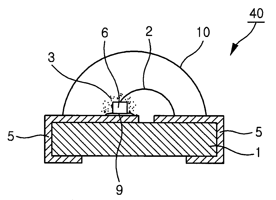
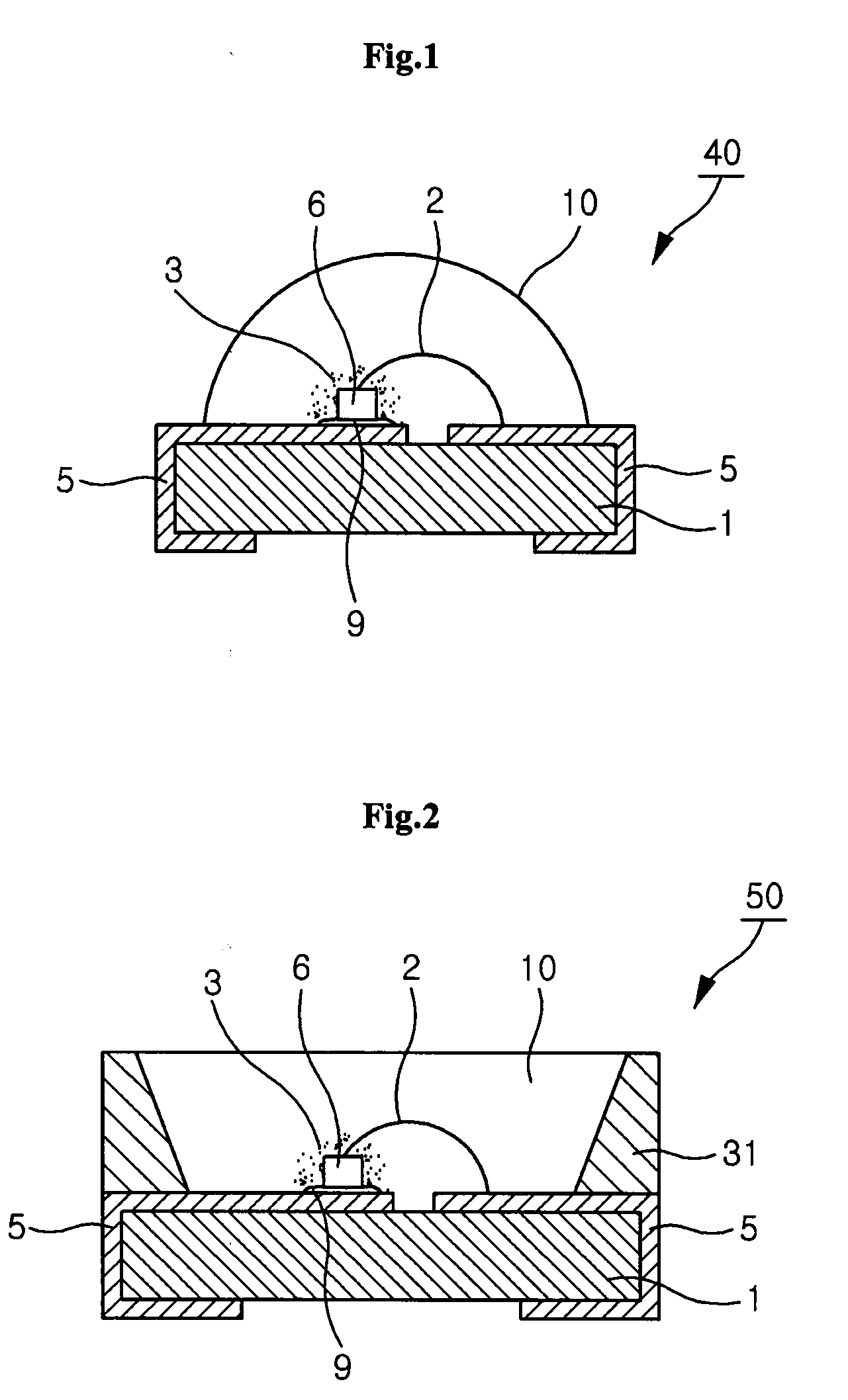
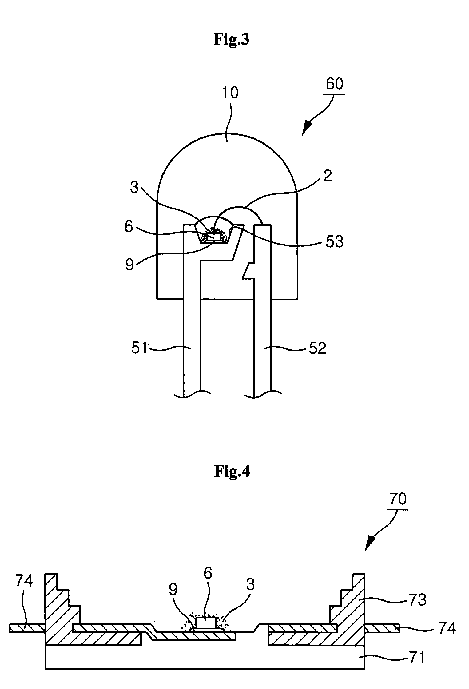
The present invention relates to a light emitting device comprising at least one light emitting diode which emits light in a predetermined wavelength region, copper-alkaline earth metal based inorganic mixed crystals activated by rare earths, which include copper-alkaline earth silicate phosphors which are disposed around the light emitting diode and absorb a portion of the light emitted from the light emitting diode and to emit light different in wavelength from the absorbed light.

Description

BACKGROUND OF THE INVENTION[0001]1. Field of the Invention[0002]The invention relates to light emitting devices and more particularly to light emitting devices including at least one light-emitting diode and phosphor, the phosphor including copper and converting the wavelength of light which is generated from a light-emitting diode.[0003]2. Description of the Related Art[0004]Light emitting diodes (LEDs), which have been used for electronic devices, are recently used for automobiles and illumination products. Since light emitting devices have superior electrical and mechanical characteristics, demands for light emitting devices expected to be increased. In connection to this, interests in white LEDs are increasing as an alternative to fluorescent lamps and incandescent lamps.[0005]In LED technology, solution for realization of white light is proposed variously. Normally, realization of white LED technology is to put the phosphor around the light-emitting diode, and mix a part of pri...

Claims


Application Information

Patent Timeline
IPC IPC(8): H01L31/12H01L33/32H01L33/50H05B44/00
CPCC09K11/663C09K11/7734H01L2224/73265H01L2224/49107H01L2224/48247H01L2224/48137H01L2224/48091H01L33/502H05B33/10H01L2224/32245H01L2924/00C09K11/661H01L25/0753H01L27/15H05B33/14H05B45/40H05B45/37H05B45/00H05B45/42C09K11/77922C09K11/77342H01L2924/00014
Inventor ROTH, GUNDULATEWS, WALTERLEE, CHUNG-HOON
Owner SEOUL SEMICONDUCTOR
Learn More