Polishing Composition for Silicon Wafer

a technology of polishing composition and silicon wafer, which is applied in the direction of electrical equipment, chemical instruments and processes, other chemical processes, etc., can solve the problems of reducing the characteristics of semiconductor devices manufactured by using the wafer, deteriorating the quality of silicon wafers, and high purification of polishing compositions, etc., to inhibit metal contamination, high removal rate, and high removal rate

Inactive Publication Date: 2009-05-21
NISSAN CHEM IND LTD
View PDF6 Cites 15 Cited by
  • Summary
  • Abstract
  • Description
  • Claims
  • Application Information

AI Technical Summary

Benefits of technology

[0023]According to the present invention, it was found that the addition of at least one compound selected from the polyaminopolycarboxylic acid compound having hydroxy group and the salts thereof to a silica-containing polishing composition exerts an effect of inhibiting metal contamination, particularly copper contamination into silicon wafers and on the surface thereof while maintaining a high removal rate. In particular, as the polishing composition exerts an effect also for amines, copper contamination can be inhibited while maintaining a high removal rate. Further, as it is not required to increase the purity of the polishing composition, metal contamination can be inhibited in a low cost.

Problems solved by technology

However, the alkaline silica-containing polishing composition contains trace amounts of metal impurities.
It becomes clear that the metal impurities diffused into the crystal cannot be removed by subsequent cleaning, thereby causing deterioration in qualities of the silicon wafer and lowering in characteristics of semiconductor device manufactured by using the wafer.
However, the high purified polishing composition is generally expensive and therefore cost for polishing presents a problem.
In addition, even when a composition having a high purity is used, in an actual polishing, metal contamination from a polishing pad, a polishing apparatus or piping system is unavoidable.
Therefore, even in case where a composition having a high purity is prepared, it is difficult to prevent metal contamination on semiconductor wafer.
This has been acknowledged as a problem.

Method used


Image

  • Polishing Composition for Silicon Wafer
  • Polishing Composition for Silicon Wafer
  • Polishing Composition for Silicon Wafer

Examples


example 1

[0034]A silica sol [silica concentration: 3.0 mass %, average particle diameter: 45 nm, copper concentration (hereinafter referred to as Cu concentration): 5 mass ppb, adjusted to pH 9 with sodium hydroxide (hereinafter referred to as NaOH)] was prepared as a base material of polishing composition (hereinafter referred to as polishing solution), and was compulsorily contaminated with copper by adding a standard copper solution for atomic absorption spectrometry analysis (copper nitrate solution having Cu concentration of 1000 mass ppm) in the silica sol so as to have Cu concentration of 10 mass ppb.

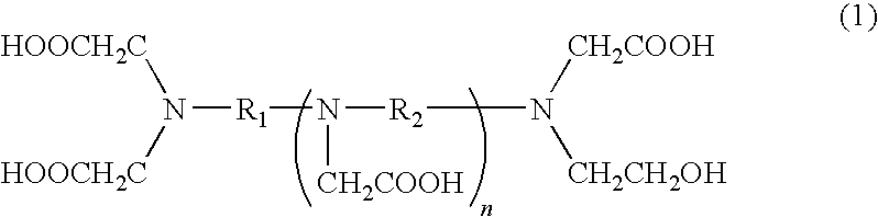
[0035]In the silica sol contaminated with copper as mentioned above, NaOH and N-(2-hydroxyethyl)ethylenediamine triacetic acid (hereinafter referred to as HEDTA) were added so as to have a concentration of 0.1 mass % and 0.1 mass %, respectively to prepare a polishing solution.

[0036]P type (100) semiconductor silicon wafer was polished for 30 minutes by using the polishing solution. For p...

example 2

[0038]A polishing solution was prepared by adding in the silica sol contaminated with copper similar to that in Example 1, NaOH and HEDTA so as to have a concentration of 0.1 mass % and 0.05 mass %, respectively. Polishing was carried out for 30 minutes by using the polishing solution, and quantitative analysis of copper was carried out.

example 3

[0039]A polishing solution was prepared by adding in the silica sol contaminated with copper similar to that in Example 1, NaOH and HEDTA so as to have a concentration of 0.1 mass % and 0.5 mass %, respectively. Polishing was carried out for 30 minutes by using the polishing solution, and quantitative analysis of copper was carried out.


PUM

PropertyMeasurementUnit
average particle diameteraaaaaaaaaa
particle diameteraaaaaaaaaa
temperatureaaaaaaaaaa

Abstract

The present invention relates to a polishing composition for silicon wafer comprising silica, a basic compound, a polyaminopolycarboxylic acid compound having hydroxy group, and water. The polishing composition can prevent metal contamination by nickel, chromium, iron, copper or the like, particularly copper contamination in polishing of silicon wafer.

Description

TECHNICAL FIELD[0001]The present invention relates to a polishing composition that makes possible to prevent efficiently metal pollution on silicon wafers.BACKGROUND ART[0002]In general, the production process of semiconductor silicon wafer comprises a slicing step of slicing a single crystal ingot to obtain a wafer in the form of thin disc, a chamfering step of chamfering the periphery of the wafer obtained in the slicing step in order to prevent cracks and break of the wafer, a lapping step of planing the chamfered wafer, an etching step of removing process strain remaining in the chamfered and lapped wafer, a polishing step of mirror-polishing the etched wafer surface and a cleaning step of cleaning the polished wafer to remove abrasives or foreign materials adhered thereto.[0003]In the above-mentioned polishing step, generally polishing is carried out by using a polishing composition obtained by dispersing fine abrasive of silica in water and further adding chemical polishing ac...

Claims


Application Information

Patent Timeline
Patent Type & Authority Applications(United States)
IPC IPC(8): C09K13/02C09K13/00
CPCC09G1/02H01L21/02024C09K3/1463
Inventor KASHIMA, YOSHIYUKIOHSHIMA, MASAAKIISHIMIZU, EIICHIROUSUEMURA, NAOHIKO
Owner NISSAN CHEM IND LTD
Why Eureka
Try Eureka