Display unit and method of manufacturing the same

Active Publication Date: 2009-04-23
SONY CORP
View PDF4 Cites 18 Cited by
  • Summary
  • Abstract
  • Description
  • Claims
  • Application Information

AI Technical Summary

Benefits of technology

[0011]However, in the above-mentioned disclosure, since the relay portion 62a is not made of a low resistance metal, wiring resistance increases more than a little so that there is a possibility of signal transmission delay for a larger screen.
[0014]In view of the above-mentioned drawbacks, it is desirable to provide a display capable of reducing the wiring resistance of a divided wiring to improve the image quality, and a method of manufacturing the same.
[0017]In the display unit of the embodiment of the present invention, since the first layer and the second layer made of a material of a higher melting point than the first layer are in direct contact with each other, the resistance of the crossing portion is reduced. This allows the divided wiring to reduce its wiring resistance, thereby suppressing a distortion of signal waveform and transmission delay of signals, etc., so as to improve the image quality.

Problems solved by technology

However, in the above-mentioned disclosure, since the relay portion 62a is not made of a low resistance metal, wiring resistance increases more than a little so that there is a possibility of signal transmission delay for a larger screen.
However, when the disclosure is applied to the above-mentioned divided wiring, there appears the resistance component in each relay portion, thereby the low resistance feature of the lower layer is scarcely used efficiently as if it were solely configured by the upper refractory metal.
As a result, it is difficult to sufficiently reduce the wiring resistance, which results in a distortion of signal waveform and transmission delay of signals, thereby leading to unevenness and degradation of image quality.
In that case, low resistance materials such as aluminum (Al) may not be used even when it is covered with a refractory metal because there may be a shortcoming of thermal resistance or diffusion in high temperatures.

Method used


Image

  • Display unit and method of manufacturing the same
  • Display unit and method of manufacturing the same
  • Display unit and method of manufacturing the same

Examples


first embodiment

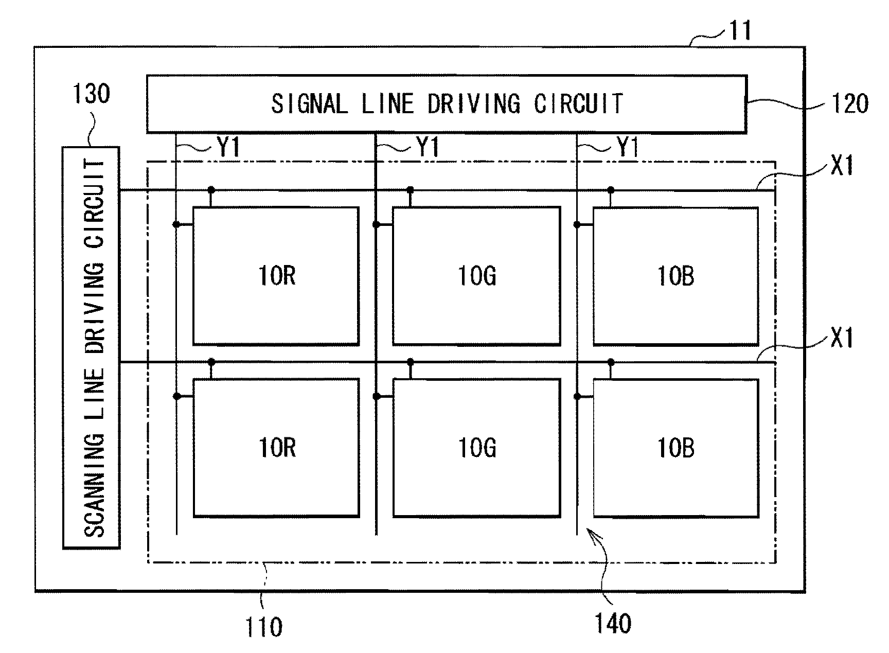
[0040]FIG. 1 shows a configuration of display unit according to a first embodiment of the present invention. The display unit is used as an ultrathin color organic EL display and so on, and is typically configured in such a manner that a display region 110, which is constituted from an after-mentioned plurality of organic light emitting elements 10R, 10G and 10B arrayed in matrix, is disposed on an insulating substrate 11 made of a glass or a plastic, while a signal line driving circuit 120 and a scanning line driving circuit 130, which are drivers for video display, are formed around the display region 110.

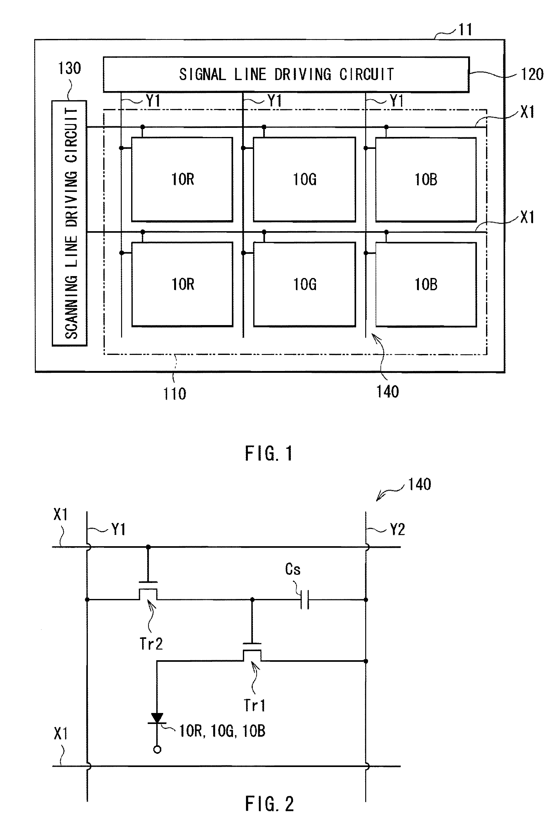
[0041]A pixel driving circuit 140 is formed in the display region 110. A plurality of gate wirings X1 are arranged in rows and a plurality of source signal lines Y1 are arranged in columns on the pixel driving circuit 140. Each intersection between the respective gate wirings X1 and the source signal lines Y1 corresponds to any one of the organic light emitting elements 10R, 10G,...

second embodiment

[0084]FIG. 10 is a cross-sectional configuration of a crossing portion 160 constituting a source signal line Y1 provided in a display unit according to a second embodiment of the present invention. The present embodiment is the same as that of the first embodiment except for adding a third layer 163 between an insulating substrate 11 and a first layer 161 so that the crossing portion 160 may become a three-layer structure. Thus, hereinbelow, component elements corresponding to those in the first embodiment are denoted by the same reference numerals.

[0085]The third layer 163 is provided to cover the undersurface of the first layer 161, which is made of a low resistance metal, so that the first layer 161 is reliably protected from a thermal damage given by the laser irradiation heating and pressure resistance of the gate insulating film 152 is further improved. Therefore, the third layer 163 is made of a material having a higher melting point than the first layer 161. More specificall...

third embodiment

[0088]FIG. 11 shows an example of the cross-sectional configuration when the present invention is applied to a liquid crystal display. The present embodiment is completely the same as the above-mentioned first and second embodiments except that the display element is constituted from a liquid crystal display element, and its operation and effects are also the same. Thus, component elements corresponding to those in the first and the second embodiments are denoted by the same reference numerals in description.

[0089]Although configuration of the liquid crystal display element is not limited in particular, here, as shown in FIG. 11, TFT is formed on the insulating substrate 11 corresponding to each pixel, and a planarization insulating film 42 and a pixel element electrode 43 made of ITO (indium-tin oxide) are formed thereon for example. A common electrode 45 which is made of ITO and is formed on an opposing substrate 44 made of glass etc. is arranged to face the pixel element electrod...


PUM


Abstract

A display unit includes, on an insulating substrate, a plurality of wirings formed to extend in different directions, a thin-film transistor, and a display element. At least one of the plurality of wirings is a divided wiring having a crossing portion formed at an intersection with the other of the plurality of wirings, and a main portion which is formed in a layer same as the other of the plurality of wirings with an insulating film in between and which is electrically connected to the crossing portion via an conductive connection provided in the insulating film. At least one of the main portion and the crossing portion includes a first layer and a second layer stacked in order from the insulating substrate side, the second layer being in direct contact with the first layer and made of a material of a higher melting point than the first layer.

Description

CROSS REFERENCE TO RELATED APPLICATIONS[0001]The present invention contains subject matter related to Japanese Patent Application JP2007-272754 filed in the Japanese Patent Office on Oct. 19, 2007, the entire contents of which being incorporated herein by reference.BACKGROUND OF THE INVENTION[0002]1. Field of the Invention[0003]The present invention relates to a display unit which is suitably applied to an organic electro luminescence display or liquid crystal display for example, and also relates to a method of manufacturing the same.[0004]2. Description of the Related Art[0005]In recent years, development of next-generation displays is active due to an increasing demand for space-saving, high luminance, low power consumption and so on. In such situation, the organic electro luminescence display (organic EL display) using an organic light emitting element attracts attention as those satisfying such demands. In the organic electro luminescence display, wide viewing angle is availabl...

Claims


Application Information

Patent Timeline
IPC IPC(8): H01L27/04H01L21/70H05B44/00
CPCH01L27/124H01L21/02675H01L21/4814H01L23/4828H01L31/1864H01L2924/01042H01L2924/13069
Inventor HAYASHI, NAOKIMAKITA, ATSUYAHIROMASU, YASUNOBU
Owner SONY CORP
Why Eureka
Try Eureka