[0011]It is an object of the invention to attain an improved saturable absorber mirror, which addresses many of those problems associated with conventional saturable absorber mirrors of the prior art, and which is
usable in lasers having high
gain active media. For passive mode-locking of lasers having a high
gain active medium, such as
fiber lasers, it is needed a saturable absorber mirror that can produce large contrast between
high intensity reflectivity and low intensity reflectivity, i.e. large modulation of reflectivity for passive mode-locking. Preferably said difference between the high and low intensity reflectivities should be at least a few percent, because the cavity losses in high gain lasers are generally quite high. This is the reason why saturable absorber mirrors designed to be used with
low gain laser media may not work properly with high gain laser media. A good
structural integrity of the saturable absorber mirror structure shall be also achieved thus minimizing nonsaturable losses. Furthermore, an efficient heat sinking of the devices shall be possible, because effective cooling is important for long-lived components, especially mode-locked laser oscillators with high average output powers. Further, it is an object of the invention to attain a method, which enable producing said improved saturable absorber mirror.
[0012]According to the first aspect of the invention it is provided a saturable absorber structure with multiple-layer epitaxial heterostructure absorbers, comprising: at least a first absorber layer of a
quantum well semiconductor QW-material with two opposite surfaces, said QW-material having a nonlinearly on
radiation intensity dependent optical absorption at a predetermined optical frequency range of an
electromagnetic radiation fed into said absorber structure in direction normal to said opposite surfaces; at least one first contacting layer of a first optically transparent semiconductor material against a surface or surfaces of said first absorber layer(s), said first contacting layer(s) having a lattice fit or a pseudomorphism with said first absorber layer(s); and a first Bragg-reflector with a plurality of quarter
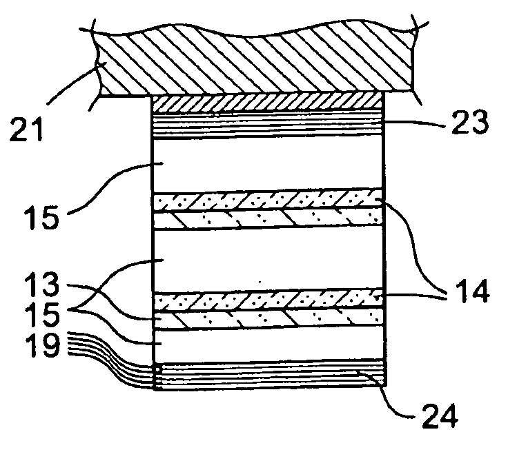
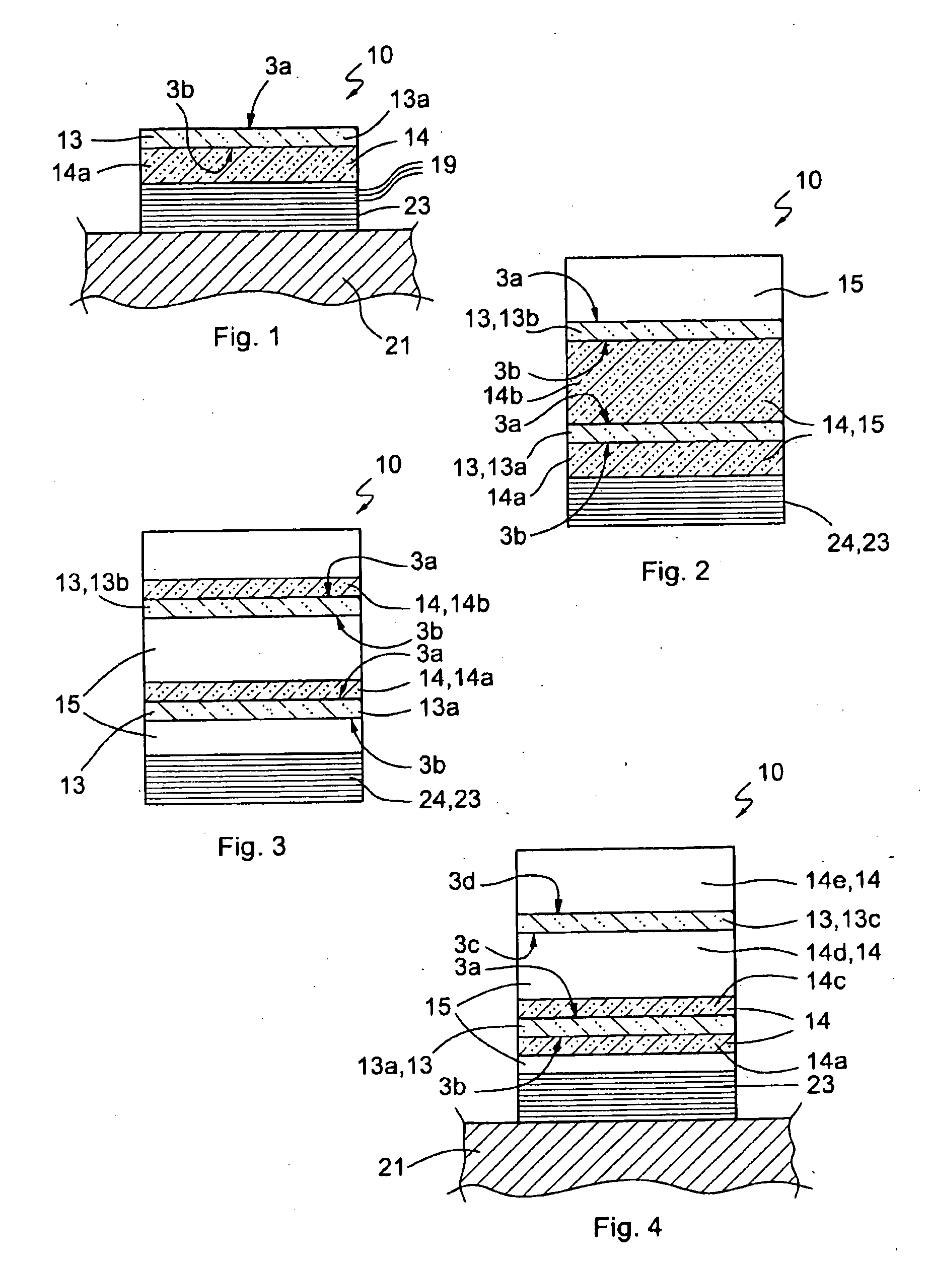
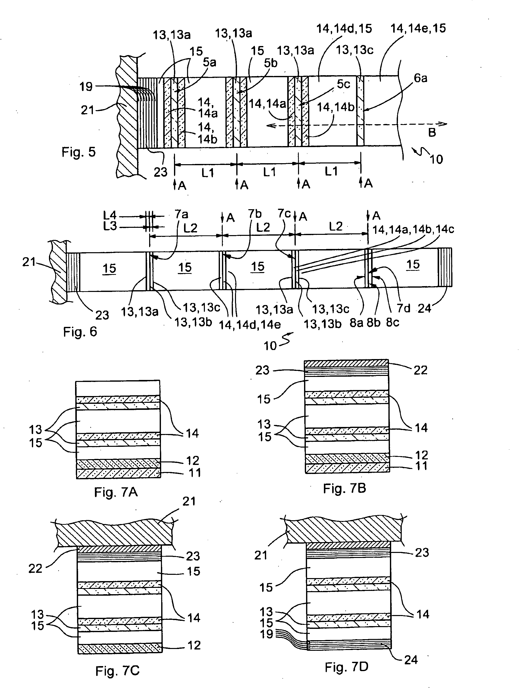
wavelength layers. Said at least one absorber layer of the QW-material has a thickness of at maximum 60 nm; and said first optically transparent semiconductor material of the contacting layer(s) is a reactive R-material, which semiconductor material contains two or more main components, at least one dopant, and at least one metallic alloying element substituting one of said main components and enhancing the incorporation of said dopant(s), said metallic alloying element having a concentration at least 50 atomic-% of that main component it substitutes; whereupon the charge carriers originating in said QW-material of the first absorber layer(s) has a first recombination time at maximum 100 picoseconds determined by recombination of the charge carriers at sites of said dopant(s), thus forming a fast saturable absorber. By this way short
charge carrier lifetimes in the saturable absorber layers can be achieved without the need to introduce dislocations or perform
ion implantation, both of which would introduce non-saturable losses and broaden the spectral features of the absorber material. Strong confinement of the photo-generated carriers in the absorber layers is achieved due to the generally large band-gap of the surrounding contacting layers of R-material. This minimizes
carrier leakage out of the absorber layers and improves the
time dynamics of the processes that result in the saturation of absorption.
[0013]One may also choose not to place the above-mentioned contacting layers around all absorber layers. In such structures two different kinds absorber layers exist, one with
fast recovery time (fast saturable absorber) and the other with slow
recovery time (slow saturable absorber). For this purpose it is provided at least a second absorber layer of a
quantum well semiconductor QW-material with two opposite surfaces, said QW-material having a nonlinearly on radiation intensity dependent optical absorption at a predetermined optical frequency range of an
electromagnetic radiation fed into said absorber structure in direction normal to said opposite surfaces; and at least one second contacting layer of an optically transparent semiconductor material against a surface or surfaces of said second absorber layer(s), said second contacting layer(s) having a lattice fit or a pseudomorphism with said second absorber layer(s), whereupon said optically transparent semiconductor material of the second contacting layer(s) is a neutral N-material, which has a lower concentration of said at least one metallic alloying element and / or a lower concentration of said at least one dopant than said R-material of the first contacting layer(s); whereupon the charge carriers originating in said QW-material of the second absorber layer(s) has a second recombination time longer than 100 picoseconds, thus forming a slow saturable absorber. The unique ability to combine slow and fast saturable absorbers in the same structure enables the optimization of
initiation and stabilization of mode locking. Further
advantage is that both slow and fast saturable absorber layers can be grown into the same structure by placement of the contacting layers.
[0014]The lattice fit or said pseudomorphism between the first contacting layer(s) and the first absorber layer(s) is arranged to be so good that said QW-material of the first absorber layer(s) has a
dislocation density at maximum 200×104 / cm2, or smaller than 10×104 / cm2, or smaller than 5×10³ / cm2: This way the point defects at the inter-faces between the contacting layers and the saturable absorber layers are distributed uniformly, and
diffusion distances of carriers to these point defects are therefore minimized. Furthermore, all structural damages are kept negligible, and the heat generated in the non-radiative recombination of carriers is also uniformly distributed, which enhances device lifetime.
[0018]The first Bragg-reflector and the optional second Bragg-reflector can be made of di-electric materials. This kind of reflectors is easier to manufacture than a semiconductor DBR due to larger
refractive index differences achieved with
dielectric materials. Typically only a few quarter layer pairs are required to achieve more than 99% reflectivity, especially when an enhancing
metal layer, such as gold or silver, is deposited on top of the last
dielectric layer. Thus, very large reflectance bandwidth can be achieved.


