Coating on a metal substrate and a coated metal product
a metal substrate and coating technology, applied in the field of coating on a metal substrate and a coated metal product, can solve the problems of large maintenance cost of metal products, time-consuming vacuum pumping period, large coating chamber, etc., and achieves simple coating, excellent wear, and chemical
- Summary
- Abstract
- Description
- Claims
- Application Information
AI Technical Summary
Benefits of technology
Problems solved by technology
Method used
Image
Examples
examples
Example to Demonstrate Known Art Problems—Laser Technology
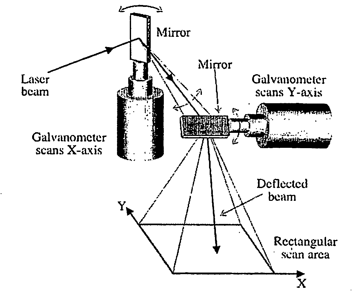
[0128]FIG. 2 represents the ITO-coating on polycarbonate sheet (˜100 mm×30 mm) produced by employing a prior art optical scanner, namely vibrating mirror (galvo-scanner), in different ITO thin-film thicknesses (30 nm, 60 nm and 90 nm). Although the ITO-coating is not deposited on metal substrate, the picture clearly demonstrates some of the problems associated with employing vibrating mirror as an optical scanner especially in ultra short pulsed laser deposition (USPLD) but also in laser assisted coatings in general. As a vibrating mirror changes its direction of angular movement at its end positions, and due to moment inertia, the angular velocity of the mirror is not constant near to its end positions. Due to vibrating movement, the mirror continuously brakes up and stops before speeding up again, causing thus irregular treatment of the target material at the edges of the scanned area. As it can be seen from FIG. 2, this in...
example of invention-1
[0133]FIG. 32a demonstrates a target material ablated with picosecond-range pulsed laser employing rotating scanner with speed accomplishing the ablation of target material with slight overlapping of adjacent pulses, avoiding the problems associated with prior art galvano-scanners. FIG. 32b shows enlarged picture of one part of the ablated material, clearly demonstrating the smooth and controlled ablation of material on both x- and y-axis and thus, generation of high quality, particle-free plasma and further, high quality thin-films and coatings. FIG. 32c demonstrates one example of possible x- and y-dimensions of one single ablation spot achieved by one or few pulses. Here, it can be clearly seen, that the invention accomplishes the ablation of material in a manner wherein the width of the ablated spot is always much bigger than the depth of the ablated spot area. Theoretically, the possible particles (if they would be generated) could now have a maximum size of the spot depth. The...
example of invention-2
[0134]FIG. 33a demonstrates an example wherein coating is carried out by employing a pico-second USPLD-laser and scanning the laser pulses with turbine scanner. Here, the scanning speed is 30 m / s, the laser spot-width being 30 μm. In this example, there is an ⅓ overlapping between the adjacent pulses.)
PUM
| Property | Measurement | Unit |
|---|---|---|
| surface area | aaaaa | aaaaa |
| surface area | aaaaa | aaaaa |
| surface area | aaaaa | aaaaa |
Abstract
Description
Claims
Application Information
 - R&D
- Intellectual Property
- Life Sciences
- Materials
- Tech Scout
- Unparalleled Data Quality
- Higher Quality Content
- 60% Fewer Hallucinations
Browse by: Latest US Patents, China's latest patents, Technical Efficacy Thesaurus, Application Domain, Technology Topic, Popular Technical Reports.
© 2025 PatSnap. All rights reserved.Legal|Privacy policy|Modern Slavery Act Transparency Statement|Sitemap|About US| Contact US: help@patsnap.com


