Eureka AIR delivers breakthrough ideas for toughest innovation challenges, trusted by R&D personnel around the world.

Method of manufacturing semiconductor storage device

a technology of semiconductor storage and manufacturing method, which is applied in the direction of semiconductor devices, basic electric elements, electrical appliances, etc., can solve the problems of difficult to form a silicon layer having a large area, the memory cell transistors to malfunction, and the variation between cells

Active Publication Date: 2009-01-01
KIOXIA CORP
View PDF12 Cites 59 Cited by
  • Summary
  • Abstract
  • Description
  • Claims
  • Application Information

AI Technical Summary

Problems solved by technology

Decrease in the on / off ratio of the channel current causes transistors of memory cells to malfunction.
However, it is difficult to form a silicon layer having a large area and good crystal properties on an insulating film, and there is the problem that variations occur between cells.
In particular, in devices on an SOI structure using solid-phase crystallization, a mismatch surface having an uncertain position is generated on an embedded insulating film.
Therefore, there is the problem that cell transistors are formed on the mismatch surface, and operation thereof become unstable.
Since a plurality of seed portions, that is, opening portions of the insulating film, are provided in the silicon substrate, occurrence of the crystal mismatch surface is inevitable.
To make room for a defective region, which may occupy 1 μm, around the center of the area of 5 μm without providing any circuit further reduces the occupying proportion of circuits, and increases the chip manufacturing cost.

Method used


Image

  • Method of manufacturing semiconductor storage device
  • Method of manufacturing semiconductor storage device
  • Method of manufacturing semiconductor storage device

Examples


first embodiment

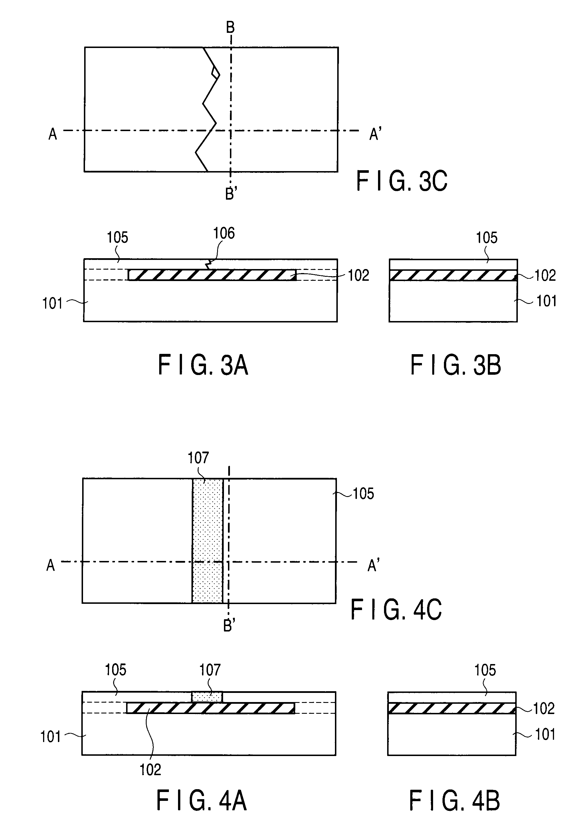
[0043]The first embodiment proposes a method of reducing defects of memory cells, by achieving position control of crystal mismatch surfaces of an SOI crystal layer, which causes problems in manufacturing an SOI structure by solid-phase crystallization.

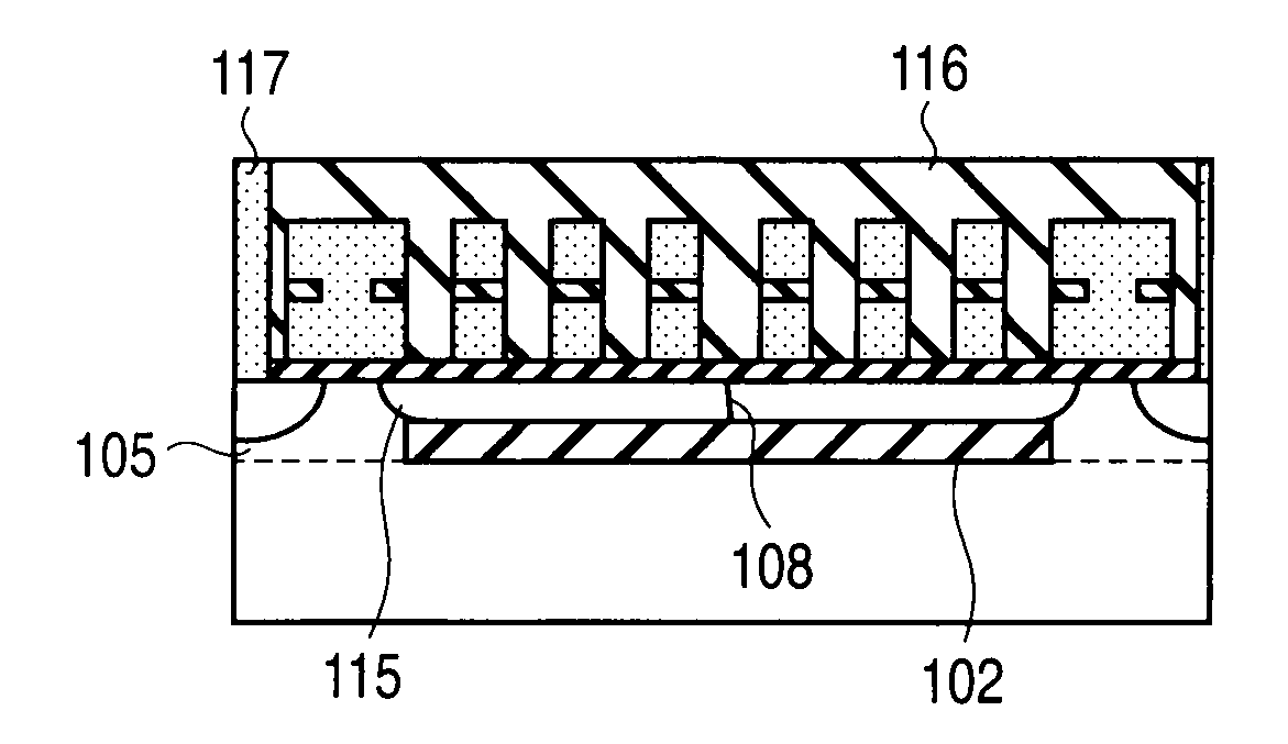
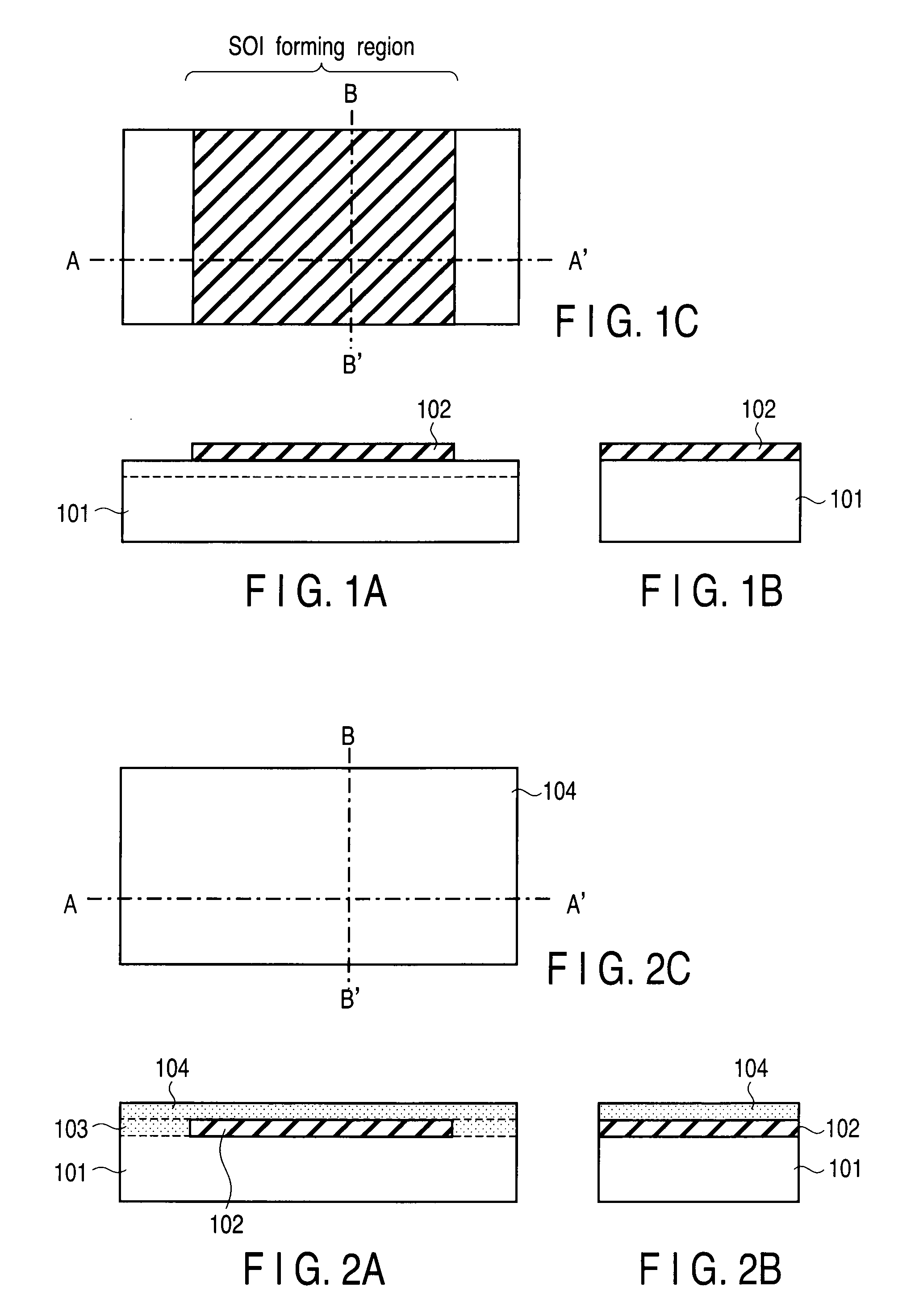
[0044]A method of manufacturing memory cell portions according to the first embodiment is explained below with reference to FIGS. 1A to 1C to FIGS. 10A and 10B. In FIGS. 1A to 1C to 10A and 10B, A is a cross-sectional view taken in a channel length direction (bit line direction), B is a cross-sectional view taken in a channel width direction (word line direction), and C is a plan view. A illustrates a cross section taken along line A-A′ of plan view C, and B illustrates a cross section taken along line B-B′ of plan view C.

[0045]First, as illustrated in FIGS. 1A to 1C, a silicon oxide film (embedded insulating film) 102 having a thickness of 50 nm is formed on a surface of a p-type single-crystal silicon substrate 101. Then, a part of ...

second embodiment

[0064]The second embodiment provides a method in which portions other than the central portion of the BOX oxide film, where a seam between solid-phase crystallizations from adjacent opening portions is expected to exist, are masked, ion implantation is performed by using oxygen, nitrogen or carbon, and thereafter solid-phase crystallization is performed, to solve the problems of prior art. Thereby, it is possible to control the position of the crystal grain boundary to fall within a region where ions are implanted.

[0065]A method of manufacturing memory cells according to the second embodiment will be explained below with reference to FIGS. 12A to 12C to FIGS. 22A to 22C. In FIGS. 12A to 12C to FIGS. 22A to 22C, A is a cross-sectional view taken in the channel length direction (bit line direction), B is a cross-sectional view taken in the channel width direction (word line direction), and C is a plan view. Further, A illustrates a cross section taken along line A-A′ in plan view C, a...

third embodiment

[0083]Although the method of the second embodiment limits the oxygen implanted region by a resist mask, the method cannot set a width of the region which limits the crystal mismatch surface to be smaller than the width which can be opened by lithography. To solve this problem, in the third embodiment, the width of the opening portions is narrowed by sidewall transfer, and thereby the position where a crystal mismatch surface is formed can be controlled to fall within a region narrower than the minimum processing width of lithography.

[0084]In the third embodiment, as illustrated in FIG. 23A, a silicon oxide film 301 having a thickness of 200 nm is deposited as a mask material on an amorphous silicon film 104, and then the silicon oxide film 301 is patterned. Thereby, a structure having an opening portion having a width of 30 nm is formed. If ion implantation is performed in this state, the same structure as in the second embodiment is achieved.

[0085]Next, as illustrated in FIG. 23B, ...


PUM


Abstract

A method of manufacturing a semiconductor storage device includes providing an opening portion in a plurality of positions in an insulating film formed on a silicon substrate, and thereafter forming an amorphous silicon film on the insulating film, in which the opening portions are formed, and in the opening portions. Then, trenches are formed to divide the amorphous silicon film, in the vicinity of a midpoint between adjacent opening portions, into a portion on one opening portion side and a portion on the other opening portion side. Next, the amorphous silicon film, in which the trenches are formed, is annealed and subjected to solid-phase crystallization to form a single crystal with the opening portions used as seeds, and thereby a silicon single-crystal layer is formed. Then, a memory cell array is formed on the silicon single-crystal layer.

Description

CROSS-REFERENCE TO RELATED APPLICATIONS[0001]This application is based upon and claims the benefit of priority from prior Japanese Patent Application No. 2007-167999, filed Jun. 26, 2007, the entire contents of which are incorporated herein by reference.BACKGROUND OF THE INVENTION[0002]1. Field of the Invention[0003]The present invention relates to a method of manufacturing a semiconductor storage device in which memory cells are formed on a silicon-on-insulator (SOI) structure.[0004]2. Description of the Related Art[0005]In structures of memory cell portions of conventional nonvolatile semiconductor storage devices, making finer memory cells has limitations for the following reason. Specifically, when the channel length of memory cells is set to 50 nm or less, the on / off ratio of the channel current decreases due to the short channel effect. Decrease in the on / off ratio of the channel current causes transistors of memory cells to malfunction.[0006]Therefore, recently, methods of fo...

Claims


Application Information

Patent Timeline
IPC IPC(8): H01L21/20
CPCH01L21/76264H01L21/84H01L27/115H01L29/66825H01L27/11524H01L27/1203H01L27/11521H10B41/35H10B69/00H10B41/30
Inventor SUZUKIISHIDA, HIROKAZUMIZUSHIMA, ICHIROOZAWA, YOSHIOAISO, FUMIKISEKINE, KATSUYUKINAKAO, TAKASHISAITO, YOSHIHIKO
Owner KIOXIA CORP
Why Eureka
Eureka Blog
Learn More