Nano engineered photo electrode for photoelectrochemical, photovoltaic and sensor applications
a photoelectrochemical and photovoltaic technology, applied in the direction of electrochemical generators, cell components, energy input, etc., can solve the problems of low solar to hydrogen (sth) conversion efficiency, exceptionally underperformance in this direction, and severely diminish the competitiveness of existing technologies, so as to minimize electron-hole recombination, the effect of unique photo sensitivity or photon energy conversion efficiency and potential optimum energy conversion efficiency
- Summary
- Abstract
- Description
- Claims
- Application Information
AI Technical Summary
Benefits of technology
Problems solved by technology
Method used
Image

Examples
example 1
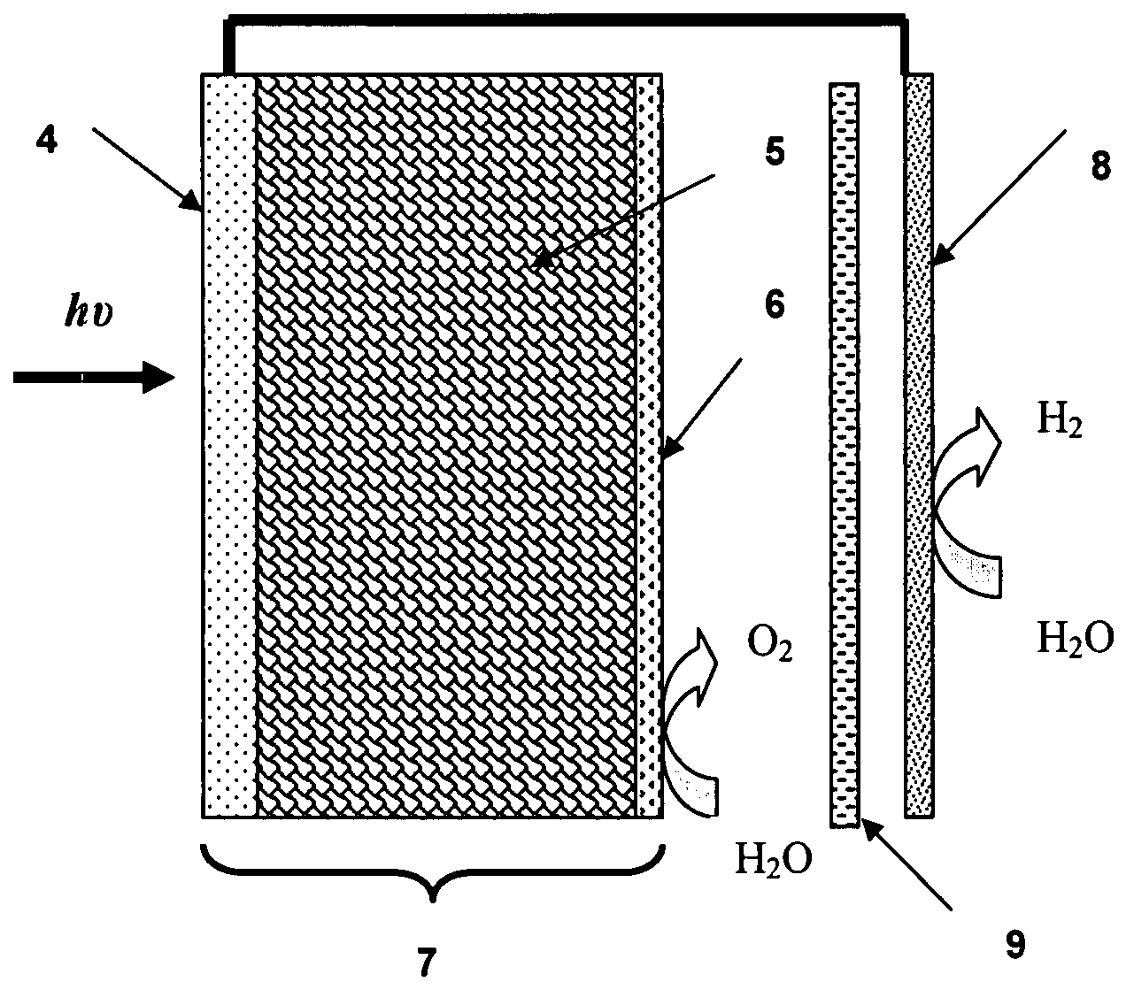
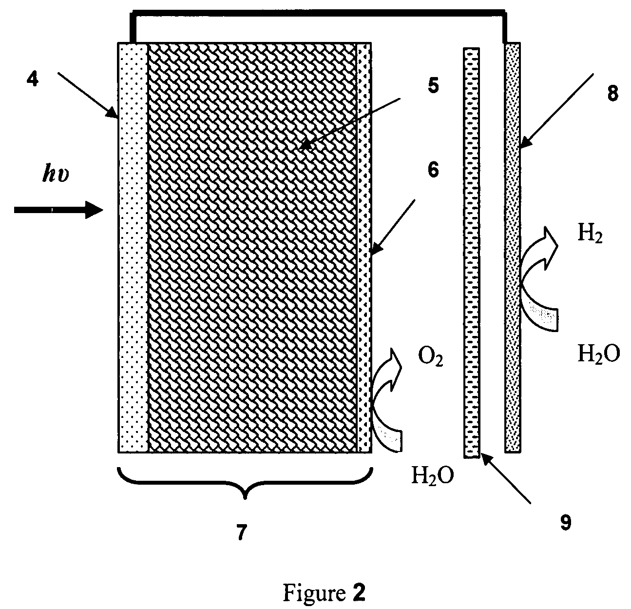
[0051]An example of the nano-engineered PEC anode of stack 7 in FIG. 4 is F—SnO / C—WO3-Nafion. The bias voltage applied can be set at a value lower than 1.2V for continuous solar simulator or sunlight operation. Scanning bias voltage in a range of 0-1.4V is used for PEC I-V data collection under 1.5 AM standard solar irradiation condition. In one specific embodiment, the structure of the assembled PEC cell using the nano engineered photo electro anode comprises:
[0052]glass / / F—SnO / C—WO3-Nafion / thin porous film / Pt gauze.
The thicknesses of the respective layers are approximately: 2 mm / 2μ / 4μ / 10 μm / 200 μm, respectively, for optimum sunlight or solar simulator illumination. More specifically, the fine structure of the UNPC in stack 7 shows nano crystalline photo active sites whose sizes are in the range of 20000-125000 nm3 and dimensions on each side are in the range of 25-50 nm. They are directly in contact with a layer of 2-6 nm carrier mobility promoters as demonstrated in FIG. 8.
[0053]...
example 2
[0057]Application of the nano engineered PEC anode on photovoltaic electrode is another embodiment of the current invention as shown in FIG. 3. This application integrates at least one of the following solar cell types: copper indium diselenide (CuInSe2), copper indium gallium diselenide (CIGS), amorphous silicon (a-Si), III-V (GaAs, InP etc), cadmium telluride (CdTe), crystalline silicon (c-Si), thin film silicon (thin-Si), or variations and combinations thereof. Furthermore, in certain embodiments, the integrated PEC photovoltaic electrode has multiple junctions including two junctions, three junctions and more junctions wherein sufficient voltage is generated for solar to hydrogen conversion.
PUM
 Abstract
Description
Claims
Application Information
 - R&D
- Intellectual Property
- Life Sciences
- Materials
- Tech Scout
- Unparalleled Data Quality
- Higher Quality Content
- 60% Fewer Hallucinations
Browse by: Latest US Patents, China's latest patents, Technical Efficacy Thesaurus, Application Domain, Technology Topic, Popular Technical Reports.
© 2025 PatSnap. All rights reserved.Legal|Privacy policy|Modern Slavery Act Transparency Statement|Sitemap|About US| Contact US: help@patsnap.com