
Image forming method and image forming apparatus

Inactive Publication Date: 2008-12-11
RICOH KK
View PDF19 Cites 27 Cited by
  • Summary
  • Abstract
  • Description
  • Claims
  • Application Information

AI Technical Summary

Benefits of technology

[0056]It is an object of the present invention to provide high-quality, stable image forming apparatus and method, which are free from abnormal images, particularly afterimages, after prolonged repeated use.
[0057]In order to solve the above problems, the present inventor and others have diligently studied an apparatus for forming an image high in durability and quality, which will not affect the basic electrophotographic characteristics or develop an abnormal image upon abrasion of a photoconductor resulting from prolonged and repeated use, finding that the apparatus is provided with at least a photoconductor, a latent electrostatic image forming unit configured to form a latent electrostatic image on the photoconductor, a developing unit for developing the latent electrostatic image by using toner to form a visible image and a transfer unit configured to transfer the visible image onto a recording medium, in which the photoconductor contains as a charge generating material on a substrate crystalline titanyl phthalocyanine having a maximum diffraction peak of at least 27.2° as a diffraction peak (±0.2°) of the Bragg angle 2θ with respect to the Cu—Kα line (wavelength of 1.542 Å), having major peaks at 9.4°, 9.6°, 24.0° and also having a peak at 7.3° as a diffraction peak on the lowest angle side but not having a peak between the peak of 7.3° and that of 9.4°, and X-metal free phthalocyanine, and the photoconductor is also formed with a single-layered photosensitive layer at least containing an electron transporting material, a positive-hole transporting substance and a binder resin represented by the following General Formula (1), thus making it possible to solve the above problems and to output a favorable image without abnormal images such as an afterimage after prolonged repeated use of the photoconductor.
[0077]The electron transporting material represented by the General Formula (1) is excellent in electron transporting capacity and also quite stable against oxidative gas such as ozone and Nox. The electrophotographic process is inevitably involved in the production of ozone on the charge thereof, with the amount varied depending on the situation. Thus, a fact that the substance is stable against the above oxidative gas is quite important in obtaining a high-quality image output for a prolonged period of time.
[0080]In order to cope with the above-described fact, the present inventor and others have made various evaluations, finding that the crystalline titanyl phthalocyanine and the X-metal free phthalocyanine are used together to greatly improve the charging property, with the high sensitivity characteristics kept. Further, since the X-metal free phthalocyanine can function as a charge generating material on single use, the combined use with the crystalline titanyl phthalocyanine makes it possible to greatly improve the durability of charging property on repeated use without substantially having adverse effects on the sensitivity, when used together with an electron transporting material represented by the General Formula (1). Excellent characteristics can be obtained particularly in combination with a positive-hole transporting substance represented by the General Formula (i), thus making it possible to provide a high-quality and stable image forming apparatus, which is free of change in charging property and the occurrence of afterimages after prolonged repeated use, with excellent light-induced discharge characteristics kept, due to the resulting synergistic effects. This combination is effective in improving stable charge as compared with the sole use of the crystalline titanyl phthalocyanine and is also far more excellent in light-induced discharge characteristics than the sole use of the X-metal free phthalocyanine.

Problems solved by technology

However, these photoconductors have been now thought to be unsuitable in forming a high-quality image because of poor productivity resulting from many coating steps and a problem in which charge occurrence in a charge generating layer moves into a charge transporting layer, during which the charge is dispersed to decrease the resolution dot density.
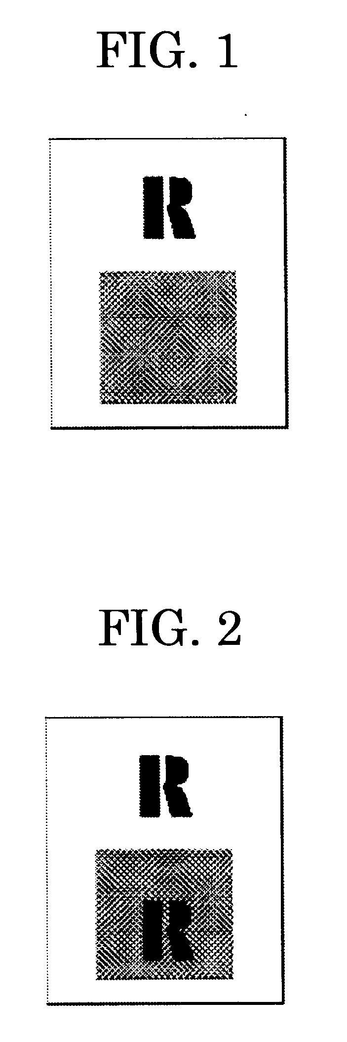
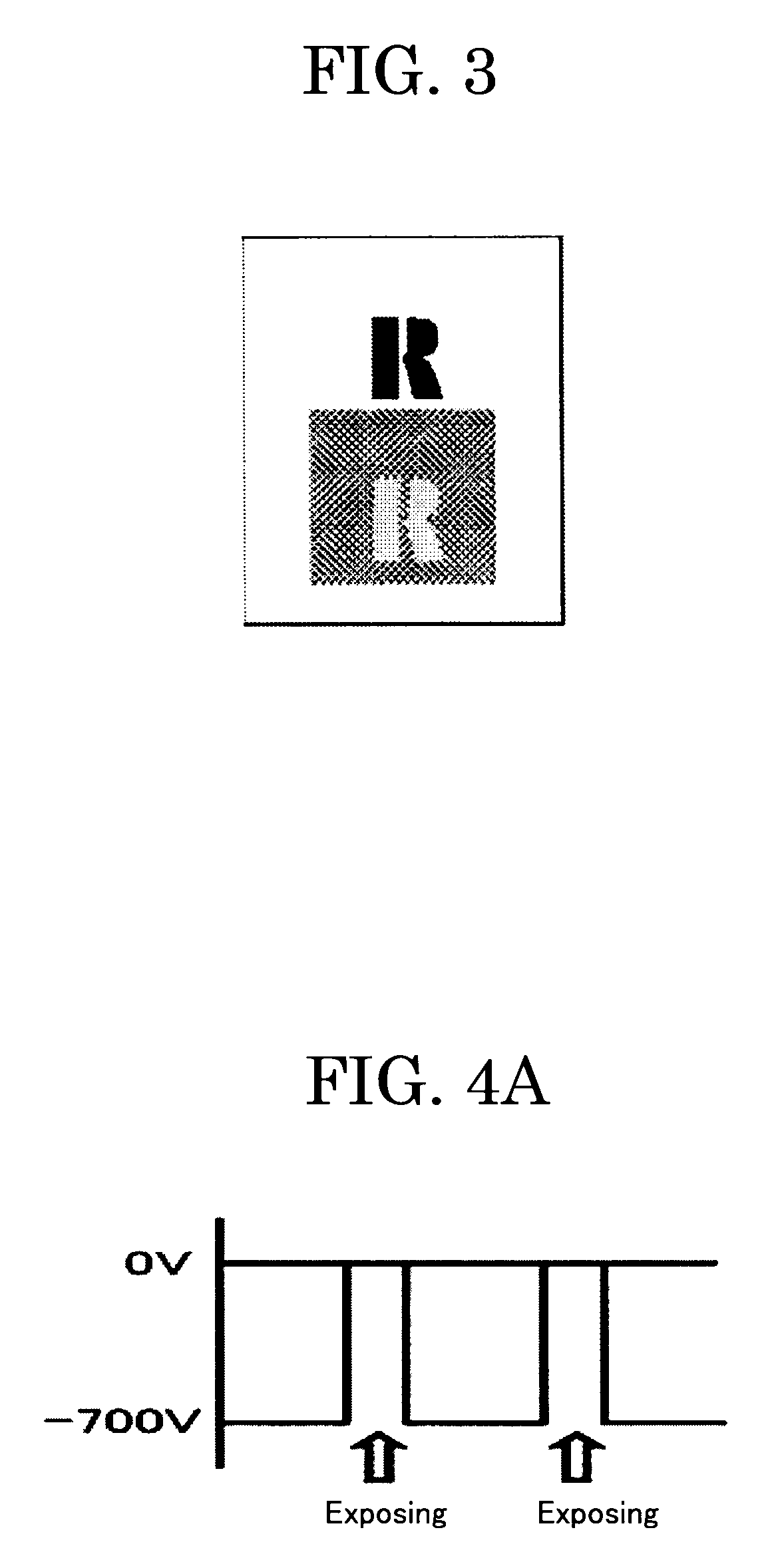
However, due to a fact that a high quality image is realized by using the photoconductors constituted with such a single layer, there is often reported a case where in an image forming apparatus for forming images at a high density, image degradation, or “afterimage,” is found as a side effect when the apparatus is repeatedly used.
It is, therefore, impossible to obtain a high-quality image output stably for a prolonged period of time as now demanded.
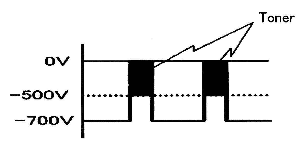
Thus an excessively enlarged dot image is perceived to be thick when viewed as a whole image, also resulting in an image on which a positive afterimage is identified.
Thus, this problem is further magnified when an image forming apparatus based on an electrophotographic process is made higher in resolution dot density.
The orientation may be combined with a specific charge generating material (azo pigment) to lower the barrier of an injection boundary surface, thus resulting in decrease in photo memory (paragraph number ).
It has been pointed out in this proposal that a thermoplastic resin is insufficient in strength and not suitable as a binder resin for the surface layer and a solvent for dissolving it on coating must be such a solvent that can easily dissolve the resin, thereby eliminating a method for dissolving a photosensitive layer (paragraph number ).
This proposal has pointed out that an electron transporting material is contained in a protective layer, thereby making it possible to decrease the remaining electric potential, but also the durability results in a disadvantage of an increased friction amount (paragraph number ).
It is now difficult to estimate certain rules on whether they are favorably combined or not.
It has been pointed out that a slow dynamic sensitivity of a photoconductor will result in a failure in complete formation of a latent image before the development and repeated use of the photoconductor will increase an afterimage.
However, if the electrons fail in quickly moving to a substrate, they remain on the charge generating layer to result in the formation of afterimages.
However, exposure before transfer would decrease a gap difference in electric potential between an exposure portion and a non-exposure portion, thus making an afterimage undistinguishable.
In order to prevent the occurrence of afterimages, we attempted to put into practical use conventional technologies described in the documents so far explained, finding that these technologies are only insufficiently applicable to an electrophotographic photoconductor intended for prints high in durability, speed and quality as well as to an image forming apparatus based on an electrophotographic process in which the above-described electrophotographic photoconductor is used.
Therefore, these technologies are unable to solve problems.

Method used


Image

  • Image forming method and image forming apparatus
  • Image forming method and image forming apparatus
  • Image forming method and image forming apparatus

Examples


production example 1

Preparation of Photoconductor 1

[0288]In a ball mill device, 27 parts by mass of an X-metal free phthalocyanine (FASTOGEN BLUE 8120BS manufactured by Dainippon Ink and Chemicals Inc.) as a charge generating material was dispersed together with 1,015 parts by mass of cyclohexanone for 120 minutes to prepare a charge generating material dispersion (1).

[0289]Separately to the above, titanyl phthalocyanine was prepared according to the method described in JP-A No. 2001-19871. Specifically, 29.2 g of 1,3-diiminoiso-indolin and 200 mL of sulfolane were mixed, and then 20.4 g of titanium tetrabutoxide was added dropwise to the mixture in a nitrogen atmosphere. After completion of the drop, the mixture was gradually heated up to 180° C. and stirred for 5 hours to react it while maintaining the reaction temperature at 170° C. to 180° C. After completion of the reaction, the resultant was naturally cooled to obtain a deposit, and then the deposit was filtered and washed with chloroform until t...

production example 2

Preparation of Photoconductor 2

[0303]A photoconductor 2 was prepared in the same manner as in Production Example 1 with the exception that the charge generating material dispersion (1) and the charge generating material dispersion (2) were added respectively at 0.38 parts by mass and 62.21 parts by mass and stirred to prepare a photosensitive layer coating solution.

production example 3

Preparation of Photoconductor 3

[0304]A photoconductor 3 was prepared in the same manner as in Production Example 1 with the exception that the charge generating material dispersion (1) and the charge generating material dispersion (2) were added respectively at 0.75 parts by mass and 61.9 parts by mass and stirred to prepare a photosensitive layer coating solution.


PUM

PropertyMeasurementUnit
Angleaaaaaaaaaa
Angleaaaaaaaaaa
Angleaaaaaaaaaa

Abstract

An image forming apparatus having at least a photoconductor, a latent electrostatic image forming unit, a developing unit, and a transfer unit, wherein the photoconductor has at least a substrate and a single-layered photosensitive layer over the substrate, and the photosensitive layer contains at least titanylphthalocyanine having specific diffraction peaks, X-metal free phthalocyanine, an electron transporting material represented by the following General Formula (1), a binder resin and a positive-hole transporting substance,where, R1 and R2 may be the same or different from each other and each represent hydrogen atom, alkyl group, cycloalkyl group, or aralkyl group; R3 to R14 may be the same or different from each other and each represent hydrogen atom, halogen atom, cyano group, nitro group, amino group, hydroxyl group, alkyl group, cycloalkyl group, or aralkyl group; and “n” represents the number of repeating units and is an integer of 0 to 100.

Description

BACKGROUND OF THE INVENTION[0001]1. Field of the Invention[0002]The present invention relates to an image forming apparatus and an image forming method suitable for copiers, facsimile machines, laser printers, direct digital plate makers and the like.[0003]2. Description of the Related Art[0004]Electrophotographic photoconductors (hereinafter sometimes referred to as “photoconductor,”“latent electrostatic image bearing member” or “image bearing member”) for use in an electrophotographic image forming apparatus applicable to copiers and laser printers and the like were predominantly inorganic photoconductors made of such material as selenium, zinc oxide or cadmium sulfide. However, organic photoconductors (OPC) that are more advantageous over such inorganic photoconductors have now found many applications in view of their reduced loads on the global environment, reduced costs, and increased flexibility in design.[0005]These organic photoconductors are broadly categorized into two typ...

Claims


Application Information

Patent Timeline
IPC IPC(8): G03G13/16G03G15/00
CPCG03G5/047G03G5/0564G03G5/0575G03G5/0637G03G5/0651G03G5/0696G03G2215/00957
Inventor KURIMOTO, EIJISHIMOYAMA, KEISUKE
Owner RICOH KK
Learn More