[0012]This invention provides a
low voltage piezoactuated storage device and process for its fabrication, equipped with an integrated large density array of nanotips made of wear-resistant conductive UNCD. Important advantages of the inventive device are:, a) the piezoactuation of the tips to make contact with the memory media, via a piezoelectric thin film, is achieved with ≦3 volts, thus providing a significant feature of driving the device with integrated complementary
metal-
oxide semiconductor (
CMOS) devices; b) the tips made of UNCD (
diamond) do not wear upon a multitude of cycles, e.g. billions of cycles, of impacting on the surface of the memory media, contrary to similar proposed devices where the tips are made of Si or other materials that are not as hard as diamond (the hardest known material); c) UNCD is the only diamond film that can be deposited at ≦400° C., which is important for achieving monolithic integration of the UNCD tips with the
CMOS driving device, since growth of diamond to fabricate the tips needs to be within the thermal budget of the
CMOS devices to avoid destruction of such; d) the piezoelectric film is deposited also with a low temperature process compatible with CMOS to enable full integration of the
hybrid piezo / UNCD large tip array with CMOS. Thus, the proposed storage device and process for its fabrication can be implemented using available technologies, resulting in a compact, portable and efficient data storage device. Desirably, the
user friendly piezoactuated storage device provides a high-density memory in the
gigabit (Gb) to
terabit (Tb) range which can be used both in government and commercial applications for stand alone memories and embedded memories for multifunctional electronic devices, such as
cell phones with image, video, and voice recording, portable movie systems, computers,
hand held electronic devices and other systems that require high-density memories in the
gigabit (Gb) to
terabit (Tb) range. It may also be useful for hard drives, disc drives or other computer storage and / or
memory functions. The inventive piezoactuated storage device and process has achieved unexpected surprisingly good results.
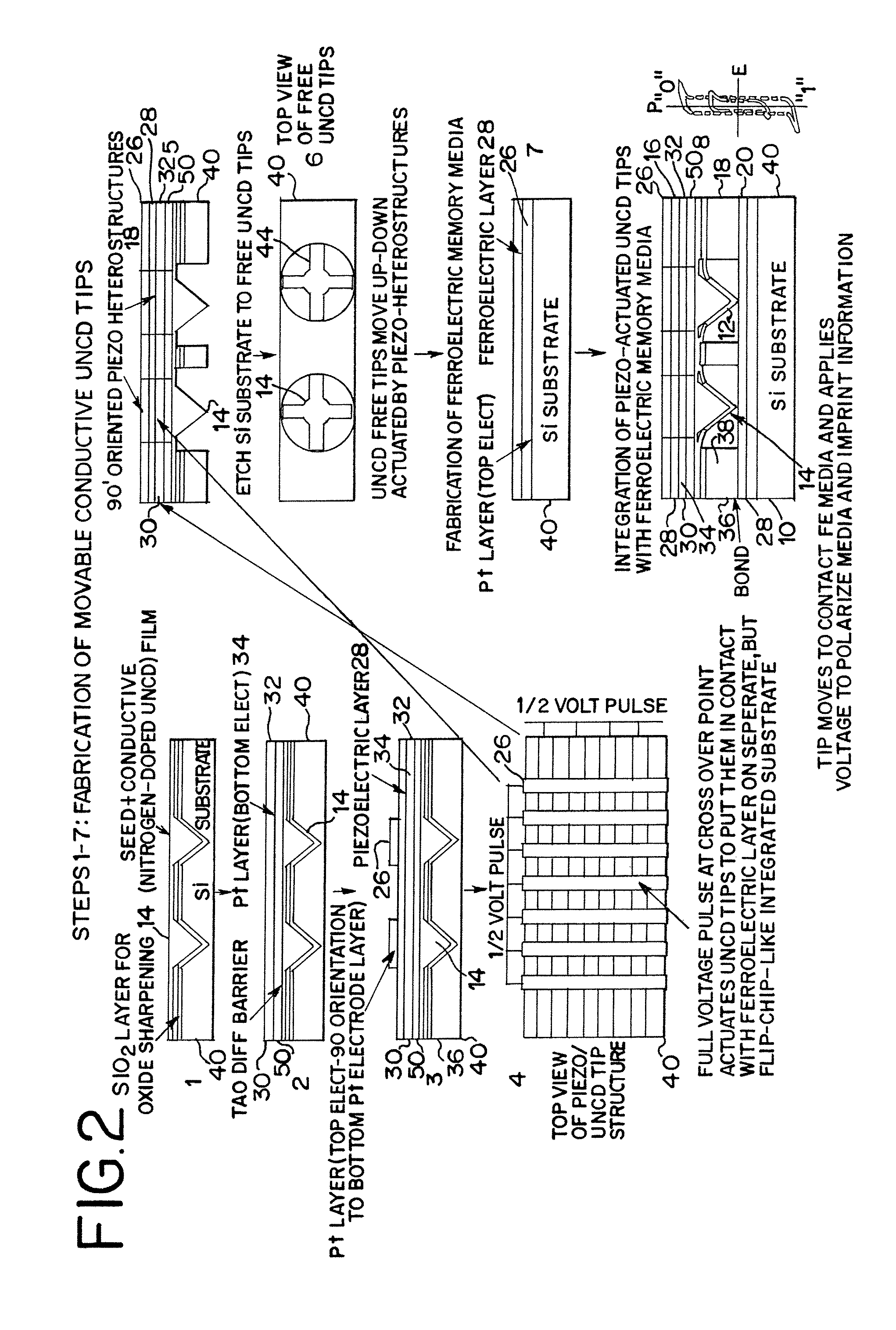
[0014]1) A piezoelectrically actuated UNCD tip array (see schematics) comprising of UNCD tips in a symmetric
square array, a Pt or other
oxidation resistant metal layer or
conductive oxide (e.g., SrRuO3) layer (bottom
electrode) on top of the tips, patterned as parallel stripes crossing over all tips in parallel rows of the
square array, a layer of piezoelectric material (e.g., Pb(ZrxTi1-x)O3 (PZT), AlN, or any other piezomaterial) grown as a
blanket film on the parallel bottom electrode stripes and on top of the UNCD layer with an
oxygen diffusion barrier film (e.g., TiAl or TaAl
alloy), to avoid chemical
etching of the UNCD
carbon layer that would be etched by
oxygen during growth of the piezolayer at high temperature in
oxygen, and finally, an array of parallel
electrically conductive stripes (similar to the bottom electrode stripes) grown on top of the piezoelectric layer, but arranged at 90° with respect to the orientation of the parallel bottom electrode stripes. This arrangement of
layers enables the application of half a
voltage on a set of parallel stripes and the other half
voltage on the 90° set of parallel stripes to achieve the full voltage, necessary for inducing polarization-piezoelectric deformation of the piezoelectric layer lattice, at the point where the bottom and top electrode strips cross on one tip. In this way, each tip can be actuated independently in a random scheme to make the tip contact the storage media on the surface of the substrate underneath the tip array.
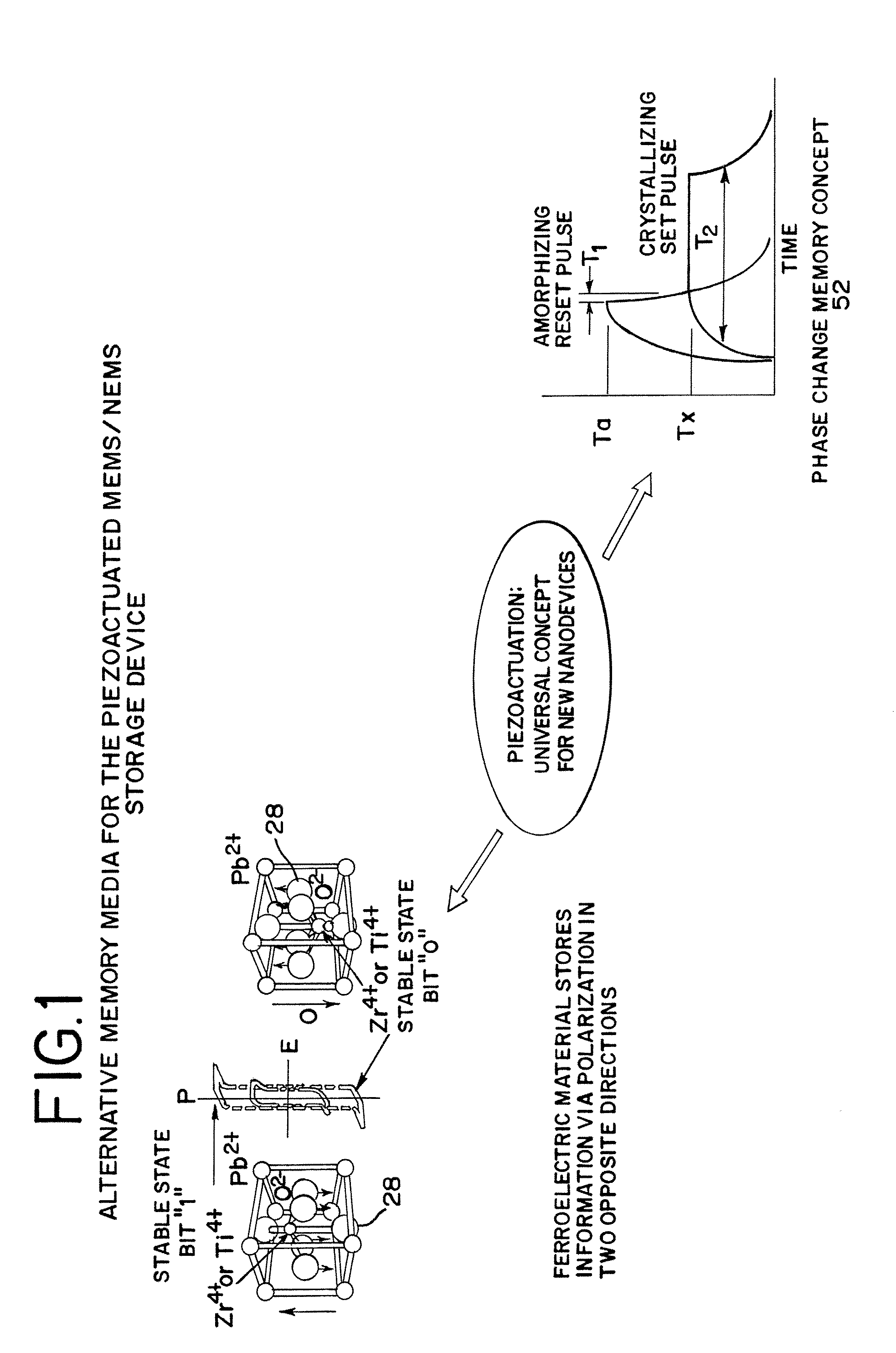
[0021]In another preferred embodiment, the memory layer of the piezoactuated storage device comprises a
phase change memory layer made a
phase change material exhibiting two orders of magnitude difference in electrical resistance between amorphous and crystalline phases. Information can be imprinted on the
phase change memory layer of the piezoactuated storage device by
current pulse-induced heating of the
phase change memory material of the memory layer. This can be accomplished by contacting the UNCD tips with the
phase change memory layer and applying a high-intensity
nanosecond duration
current pulse to the phase change memory layer. The phase of the memory layer will change from a crystalline phase to a high electrical resistance
amorphous phase in response to the high-intensity
nanosecond duration
current pulse that heats the material to high temperature (˜610° C.) and let it cool down rapidly (also in nanoseconds) to induce the amorphous state. A longer low-intensity current pulse can be applied to the phase change memory layer in order to change the phase of the memory layer from the high-electrical resistance
amorphous phase to a crystalline phase having about three orders of magnitude lower electrical resistance than the
amorphous phase. The longer lower-intensity current pulse is of a longer duration and a
lower intensity than the high-intensity
nanosecond duration current pulse. Advantageously, the piezoactuated storage device provides non-
volatile memory performance in response to the difference in resistance between the high-electrical resistance amorphous phase and the crystalline phase of the memory layer.

