Display device, driving method of display device, and electronic apparatus
a display device and driving method technology, applied in the direction of electric digital data processing, instruments, computing, etc., can solve the problems of deteriorating contrast and occurrence of cross talk, affecting and the movement of charged particles may not be perfectly inhibited, so as to reduce the gate bias, the effect of suppressing undesirable movement of charged particles and improving the write speed of images
- Summary
- Abstract
- Description
- Claims
- Application Information
AI Technical Summary
Benefits of technology
Problems solved by technology
Method used
Image

Examples
first embodiment
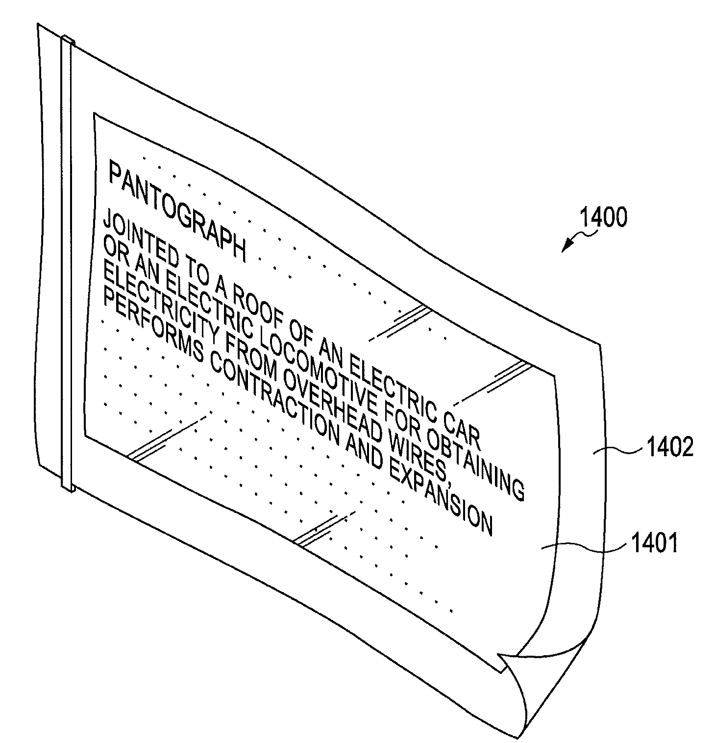
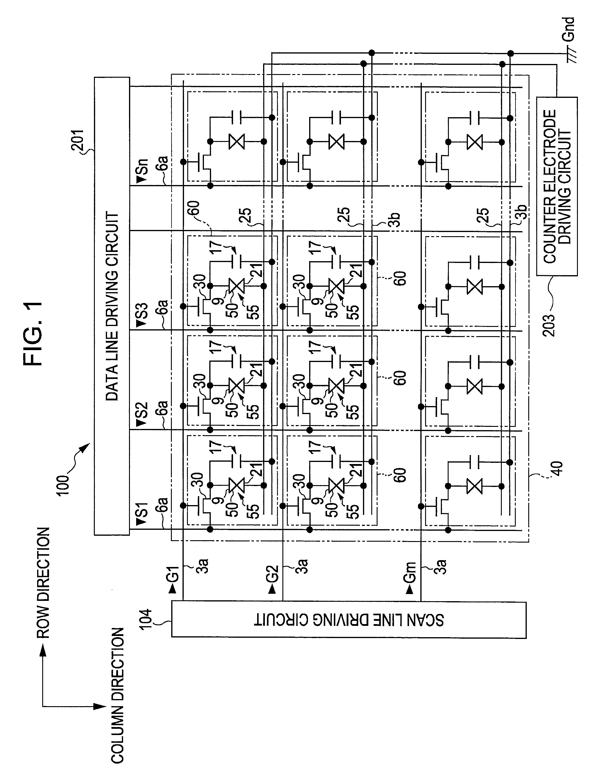
[0028]FIG. 1 is a block diagram showing an electrical structure of an electrophoresis device lo which is one embodiment of a display device of the invention. The electrophoresis device 100 according to this embodiment is an active matrix type electrophoresis display device employing organic thin film transistors (TFT) as pixel switching elements. The electrophoresis device 100 can be applied to a flexible electronic apparatus such as electronic paper.
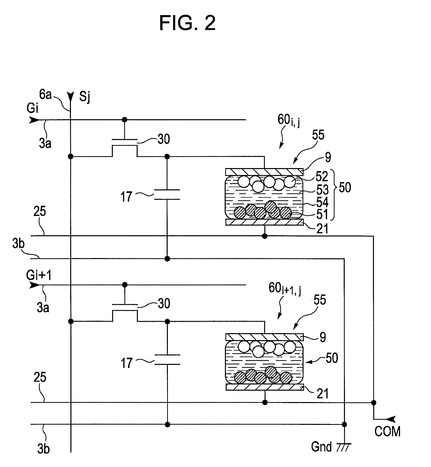
[0029]The electrophoresis device 100 includes a plurality of scan lines 3a each extending in a row direction (horizontal direction), a plurality of data lines 6a each extending in a column direction (vertical direction), and a plurality of capacitor lines 3b each extending in parallel with the scan lines 3a. Every intersection of the scan lines 3a and the data lines 6a is provided with a pixel 60 which is the unit of display. The pixels 60 are arranged in the row direction and the column direction along the scan lines 3a and the data li...
second embodiment
[0052]FIG. 7 is a timing chart illustrating driving voltages of an electrophoresis device according to a second embodiment. FIG. 7 corresponds to FIG. 3 according to the first embodiment. This embodiment is different from the first embodiment only in the waveform of the driving signals but is the same as the first embodiment in the structure thereof.
[0053]As shown in FIG. 7, in a driving method according to this embodiment, each of the scan lines is scanned two times during a period of one frame (corresponding to 1 / 60 seconds, in the case of displaying 60 frames in one second). First of all, the first time of scan signals G1, G2, G3, . . . , Gi, Gi+1, Gi+2, . . . , and Gm are supplied to the first to m-th scan lines, and the first time of image signals S1, S2, . . . , Sj, Sj+1, Sj+2, . . . , and Sn are supplied to the first to n-th data lines at timings in synchronization with the timings of supply of the scan signals G1, G2, G3, . . . , Gi, Gi+1, Gi+2, . . . , and Gm. Next, the sec...
PUM
 Abstract
Description
Claims
Application Information
 - R&D
- Intellectual Property
- Life Sciences
- Materials
- Tech Scout
- Unparalleled Data Quality
- Higher Quality Content
- 60% Fewer Hallucinations
Browse by: Latest US Patents, China's latest patents, Technical Efficacy Thesaurus, Application Domain, Technology Topic, Popular Technical Reports.
© 2025 PatSnap. All rights reserved.Legal|Privacy policy|Modern Slavery Act Transparency Statement|Sitemap|About US| Contact US: help@patsnap.com