Method for forming an ultra low dielectric film by forming an organosilicon matrix and large porogens as a template for increased porosity

a dielectric film, organosilicon technology, applied in semiconductor devices, chemical/physical/physico-chemical processes, chemical apparatus and processes, etc., can solve the problems of increasing the parasitic capacitance between devices, reducing the response time of devices, and damage to device structures

Inactive Publication Date: 2008-05-08
APPLIED MATERIALS INC
View PDF6 Cites 14 Cited by
  • Summary
  • Abstract
  • Description
  • Claims
  • Application Information

AI Technical Summary

Problems solved by technology

The high temperatures at which some thermal CVD processes operate can damage device structures having layers previously formed on the substrate.
However, the barrier / liner layers typically have dielectric constants that are greater than about 2.5, and the high dielectric constants result in a combined insulator that may not significantly reduce the dielectric constant.
Additionally, the smaller device geometries result in an increase in parasitic capacitance between devices.
Parasitic capacitance between metal interconnects on the same or adjacent layers in the circuit can result in crosstalk between the metal lines or interconnects and / or resistance-capacitance (RC) delay, thereby reducing the response time of the device and degrading the overall performance of the device.
Increasing the thickness of the dielectric materials, however, does not address parasitic capacitance within the same metallized layer or plane.

Method used


Image

  • Method for forming an ultra low dielectric film by forming an organosilicon matrix and large porogens as a template for increased porosity
  • Method for forming an ultra low dielectric film by forming an organosilicon matrix and large porogens as a template for increased porosity
  • Method for forming an ultra low dielectric film by forming an organosilicon matrix and large porogens as a template for increased porosity

Examples


examples

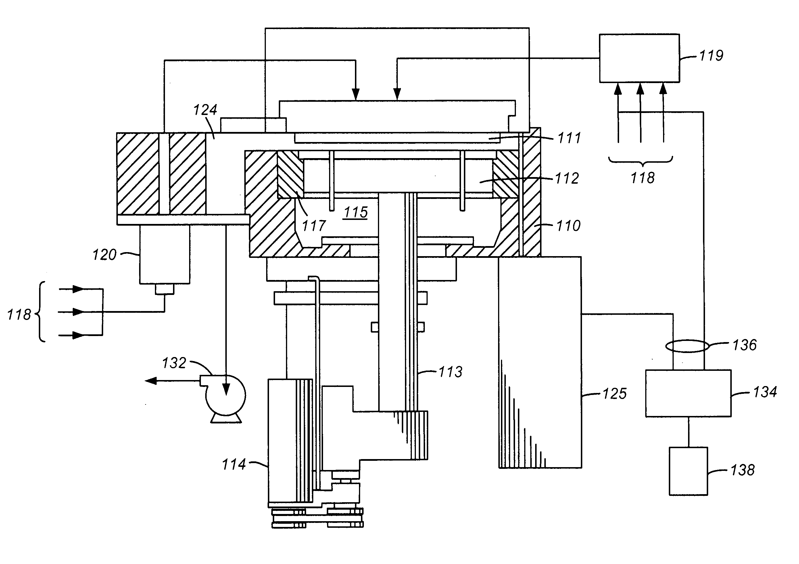
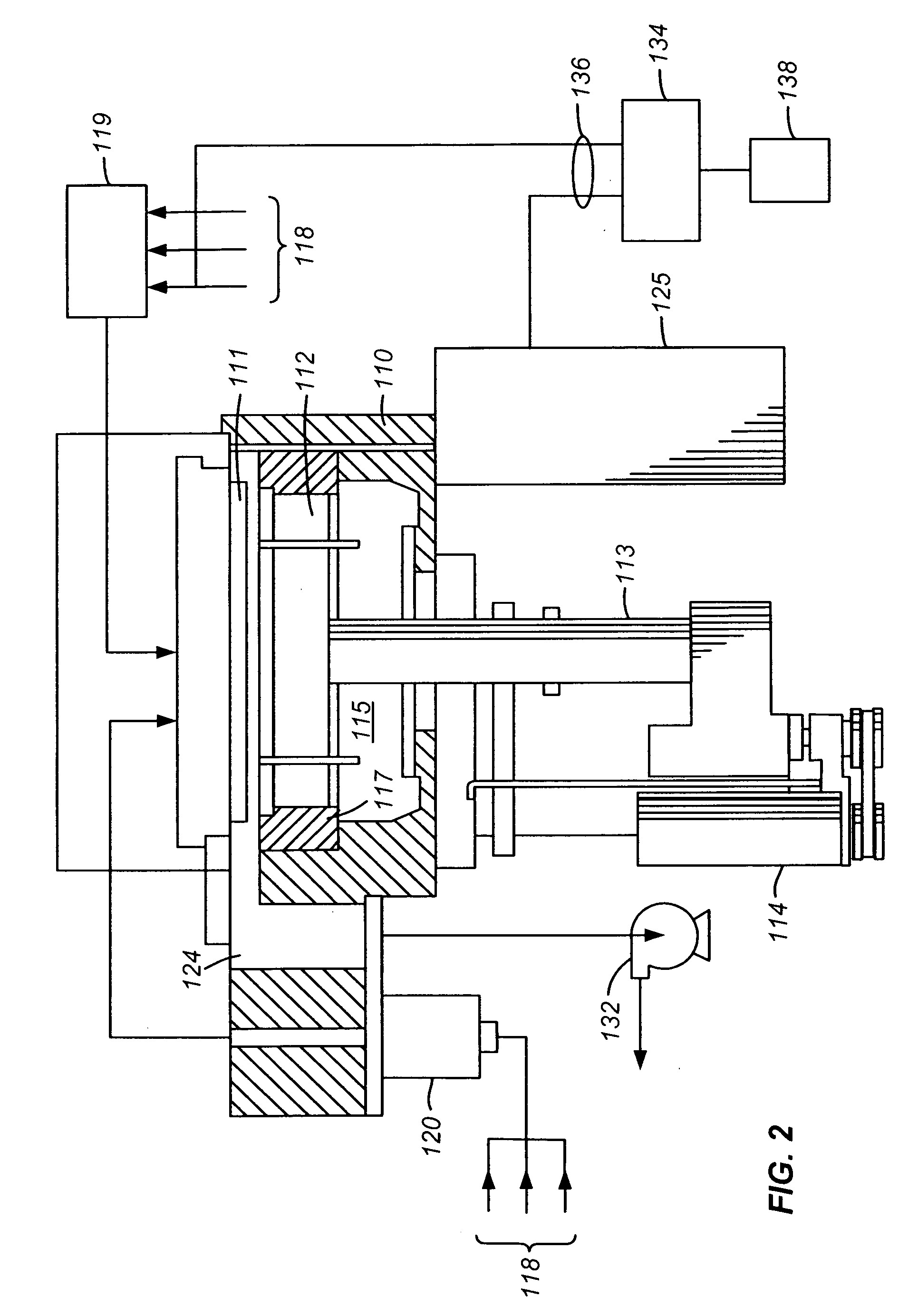
[0137] The following examples demonstrate deposition of a nano-porous silicon oxide based film having dispersed microscopic gas voids. This example is undertaken using a chemical vapor deposition chamber, and in particular, a CENTURA “DLK” system fabricated and sold by Applied Materials, Inc., Santa Clara, Calif.

Silicon Compound Having Silicon Containing and Thermally Labile Imparting Components (Hypothetical)

[0138] A nano-porous silicon oxide based film is deposited at a chamber pressure of 1.0 Torr and temperature of 30° C. from reactive gases which are vaporized and flown into the reactor as follows:

methylsilyl-2-furyl ether, at 150 sccmnitrous oxide (N2O), at1000 sccm

[0139] Prior to entering the chamber, the nitrous oxide is dissociated in a microwave applicator that provides 2000 W of microwave energy. The substrate is positioned 600 mil from the gas distribution showerhead and the reactive gases are introduced for 2 minutes. The substrate is then heated over a time period...


PUM

PropertyMeasurementUnit
feature sizesaaaaaaaaaa
dielectric constantaaaaaaaaaa

Abstract

Ultra low K nanoporous dielectric films may be formed by chemical vapor deposition of silicon-containing components and large non-silicon containing porogens having labile groups. In accordance with one embodiment of the present invention, a low K nanoporous film may be formed by the oxidative reaction between trimethylsilane (the silicon-containing component) and alpha-terpinene (the non-silicon containing component). In accordance with certain embodiments of the present invention, the oxidant can comprise other than molecular oxygen, for example water vapor introduced in-situ or remotely, and then exposed to RF energy to generate reactive ionic species.

Description

CROSS-REFERENCES TO RELATED APPLICATIONS [0001] This nonprovisional patent application claims priority to U.S. Provisional Patent Application No. 60 / 561,727, filed Apr. 12, 2004, the entire disclosure of which is incorporated herein by reference for all purposes.BACKGROUND OF THE INVENTION [0002] One of the primary steps in the fabrication of modern semiconductor devices is the formation of metal and dielectric films on a substrate by chemical reaction of gases. Such deposition processes are referred to as chemical vapor deposition or CVD. Conventional thermal CVD processes supply reactive gases to the substrate surface where heat-induced chemical reactions take place to produce a desired film. The high temperatures at which some thermal CVD processes operate can damage device structures having layers previously formed on the substrate. A preferred method of depositing metal and dielectric films at relatively low temperatures is plasma-enhanced CVD (PECVD) techniques such as describ...

Claims


Application Information

Patent Timeline
Patent Type & Authority Applications(United States)
IPC IPC(8): B01J19/00H01L21/312H01L21/316H01L21/44H01L21/768
CPCH01L21/02126H01L21/02203H01L21/02216H01L21/02274H01L21/02304H01L21/02351H01L21/76825H01L21/3122H01L21/31695H01L21/76811H01L21/76813H01L21/7682H01L21/02362H01L2221/1047
Inventor SCHMITT, FRANCIMARM'SAAD, HICHEM
Owner APPLIED MATERIALS INC
Why Eureka
Try Eureka