Manufacturing method of semiconductor device
- Summary
- Abstract
- Description
- Claims
- Application Information
AI Technical Summary
Benefits of technology
Problems solved by technology
Method used
Image

Examples
first embodiment
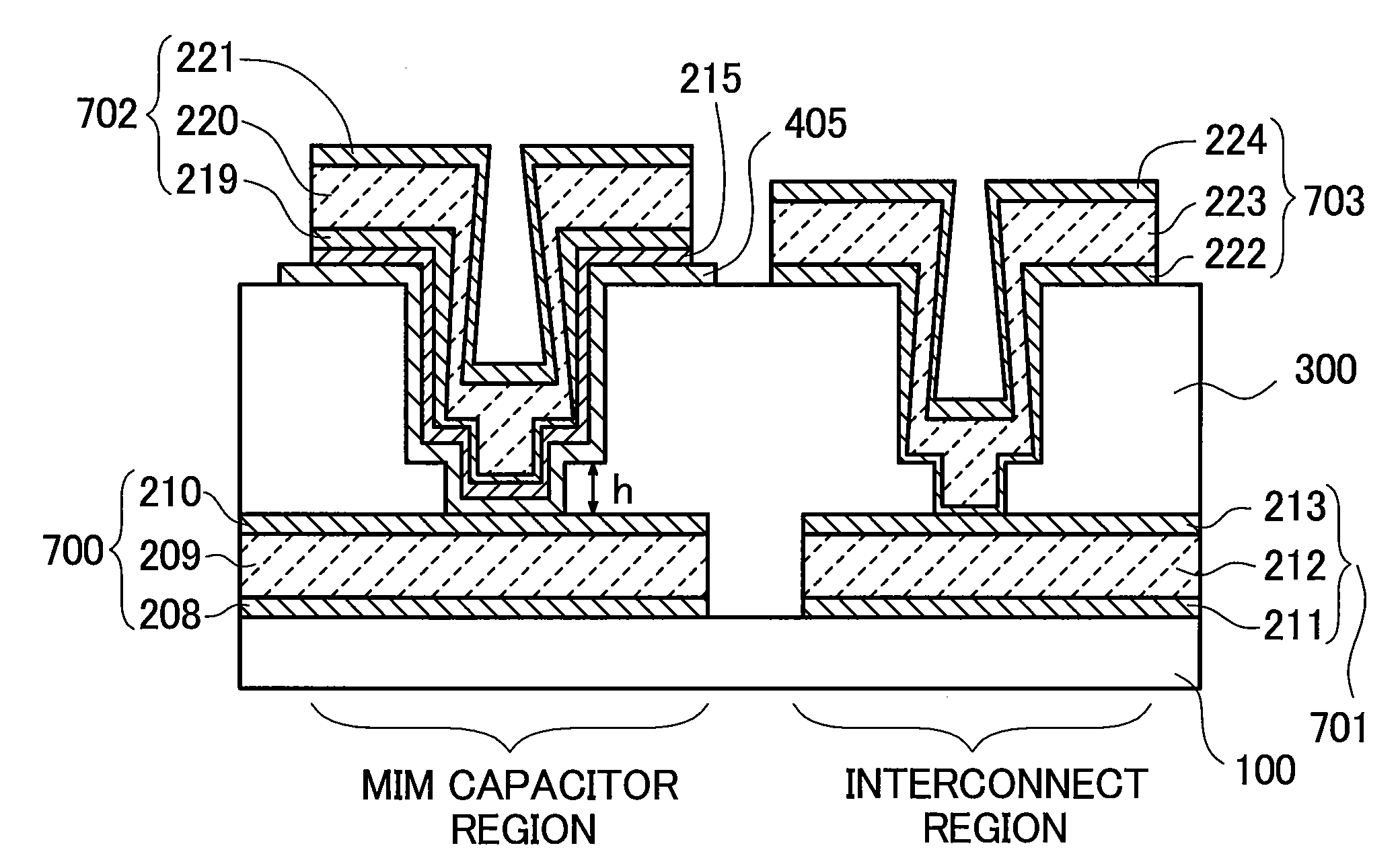
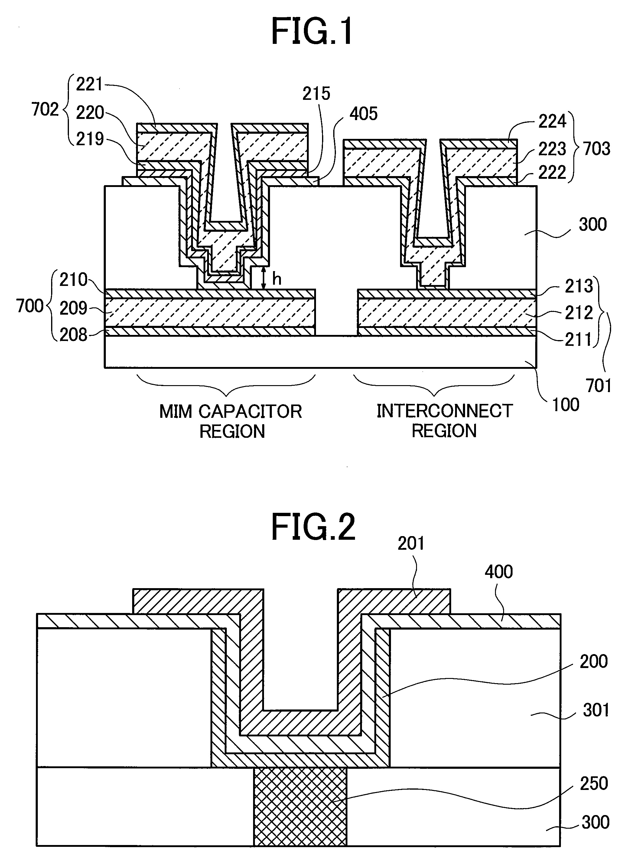
[0061]FIG. 4 and FIG. 5 are cross sectional views showing manufacturing steps of a semiconductor device according to a first embodiment of the present invention. Description is to be made successively.
[0062]After forming titanium nitride of 50 nm film thickness, aluminum of 400 nm film thickness, and titanium nitride of 50 nm film thickness by using a sputtering method on a substrate 100 formed with a semiconductor device, a first metal interconnect 700 comprising a first barrier metal 208, a first aluminum layer 209 and a second barrier metal layer 210, and a second metal interconnect 701 comprising a third barrier metal 211, a second aluminum layer 212, and a fourth barrier metal layer 213 were formed by using a lithographic method and a dry etching method. Then, a silicon oxide film of 2 μm thickness was formed by using a plasma CVD method as a first interlayer dielectric film 300. Then, after improving the planarity of the first interlayer dielectric film by using a chemical-mec...
second embodiment
[0080]This embodiment is one of application examples of the first embodiment and the embodiment is to be described with reference to cross sectional views showing the manufacturing steps of the semiconductor device shown in FIG. 9 and FIG. 10. Description is to be made successively.
[0081]After forming titanium nitride of 50 nm film thickness, aluminum of 400 nm film thickness and titanium nitride of 50 nm film thickness on a substrate 100 formed with a semiconductor device by using a sputtering method, a first metal interconnect 700 comprising a first barrier metal layer 208, a first aluminum layer 209, and a second barrier metal 210, and a second metal interconnect 701 comprising a third barrier metal layer 211, a second aluminum layer 212, and a fourth barrier metal 213 were formed by using a lithographic method and a dry etching method.
[0082]Then, a silicon oxide film of 2 μm thickness was formed by using a plasma CVD method to form a first interlayer dielectric film 300. Then, a...
third embodiment
[0098]FIG. 11 and FIG. 12 are cross sectional views showing manufacturing steps of a semiconductor device according to the invention. Description is to be made successively.
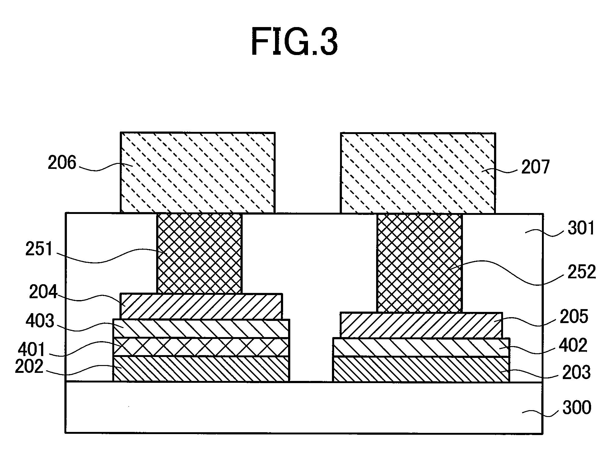
[0099]As shown in FIG. 11A, a silicon oxide film of 500 nm thickness was formed on a substrate 100 formed with a semiconductor device by using a plasma CVD method to form a first interlayer dielectric film 300. Then, a photosensitive organic polymer film was formed so as to have an opening in a region intended to form an interconnect, and a desired region of the first interlayer dielectric film 300 was removed by a dry etching method using the film as a fabrication mask. Then, after forming tantalum of 50 nm film thickness and a copper film of 100 nm thickness by a sputtering method, and after growing the copper film further by an electroplating method, excessive tantalum film and copper film on the first interlayer dielectric film 300 were removed by using a chemical-mechanical polishing method to form a fifth m...
PUM
 Abstract
Description
Claims
Application Information
 - R&D
- Intellectual Property
- Life Sciences
- Materials
- Tech Scout
- Unparalleled Data Quality
- Higher Quality Content
- 60% Fewer Hallucinations
Browse by: Latest US Patents, China's latest patents, Technical Efficacy Thesaurus, Application Domain, Technology Topic, Popular Technical Reports.
© 2025 PatSnap. All rights reserved.Legal|Privacy policy|Modern Slavery Act Transparency Statement|Sitemap|About US| Contact US: help@patsnap.com