Surface acoustic wave device and communication device
a surface acoustic wave and communication device technology, applied in the direction of impedence networks, electrical devices, electromechanical/electrostrictive/magnetostrictive devices, etc., can solve the problems of unbalanced input-balanced output type surface acoustic wave filter, input-unbalanced output, etc., to achieve high sensitivity and improve balan
- Summary
- Abstract
- Description
- Claims
- Application Information
AI Technical Summary
Benefits of technology
Problems solved by technology
Method used
Image
Examples
first embodiment
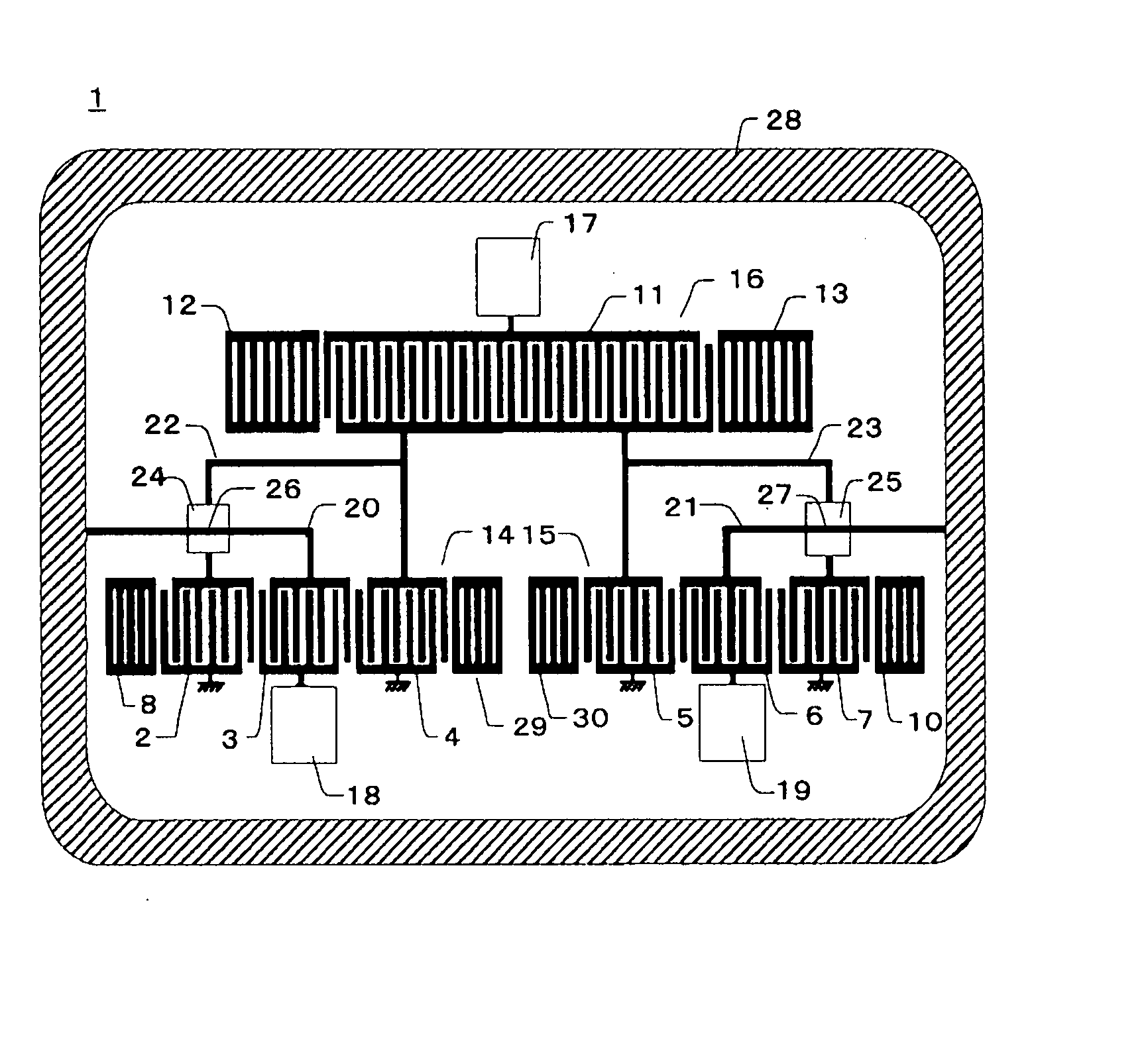
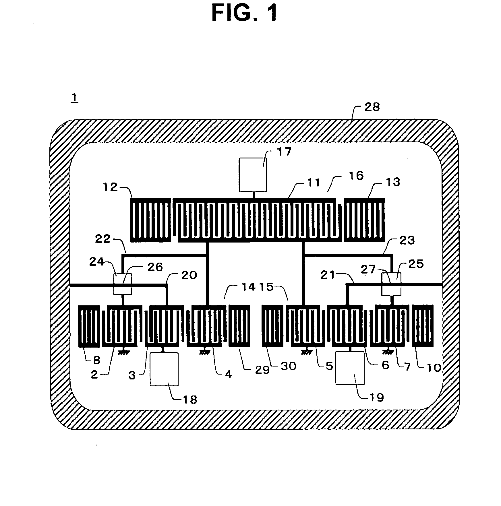
[0090] An example of manufacturing and evaluation of the surface acoustic wave device according to the first embodiment shown in FIG. 1 will be described in detail.
[0091] Fine electrode patterns made of an alloy of 99 weight % Al and 1 weight % Cu and constituting the first and second surface acoustic wave elements 14 and 15 were formed on a piezoelectric substrate (a mother substrate that is to be divided into a plurality of individual substrates) 1 made of 38.7° rotated Y-cut X-propagation single crystalline LiTaO3. The electrode patterns were formed by photolithography using a sputtering apparatus, a stepper and an RIE (Reactive Ion Etching) apparatus.
[0092] First, the piezoelectric substrate 1 was ultrasonically cleaned using acetone, isopropyl alcohol or the like to remove organic substances. After drying the piezoelectric substrate 1 sufficiently in a clean oven, a film of metal layer to make the electrodes was formed. The metal layer was formed by the sputtering apparatus u...
second embodiment
[0107] An example of manufacturing and evaluation of the surface acoustic wave device according to the second embodiment shown in FIG. 4 will be described in detail.
[0108] Fine electrode patterns made of an alloy of 99 weight % Al and 1 weight % Cu were formed on a piezoelectric substrate (a mother substrate that is to be divided into a plurality of individual substrates) 101 made of 38.7° rotated Y-cut X-propagation single crystalline LiTaO3.
[0109] The electrode patterns were formed by photolithography using a sputtering apparatus, a stepper and an RIE apparatus.
[0110] First, the piezoelectric substrate 101 was ultrasonically cleaned using acetone, isopropyl alcohol or the like to remove organic substances. After drying the piezoelectric substrate 101 sufficiently in a clean oven, a film of metal layer to make the electrodes was formed. The metal layer was formed by the sputtering apparatus using the alloy of 99 weight % Al and 1 weight % Cu as material. A thickness of the metal...
PUM
 Abstract
Description
Claims
Application Information
 - R&D
- Intellectual Property
- Life Sciences
- Materials
- Tech Scout
- Unparalleled Data Quality
- Higher Quality Content
- 60% Fewer Hallucinations
Browse by: Latest US Patents, China's latest patents, Technical Efficacy Thesaurus, Application Domain, Technology Topic, Popular Technical Reports.
© 2025 PatSnap. All rights reserved.Legal|Privacy policy|Modern Slavery Act Transparency Statement|Sitemap|About US| Contact US: help@patsnap.com


