
High-speed low-voltage programming and self-convergent high-speed low-voltage erasing schemes for EEPROM

Inactive Publication Date: 2007-07-12
YIELD MICROELECTRONICS CORP
View PDF4 Cites 10 Cited by
  • Summary
  • Abstract
  • Description
  • Claims
  • Application Information

AI Technical Summary

Benefits of technology

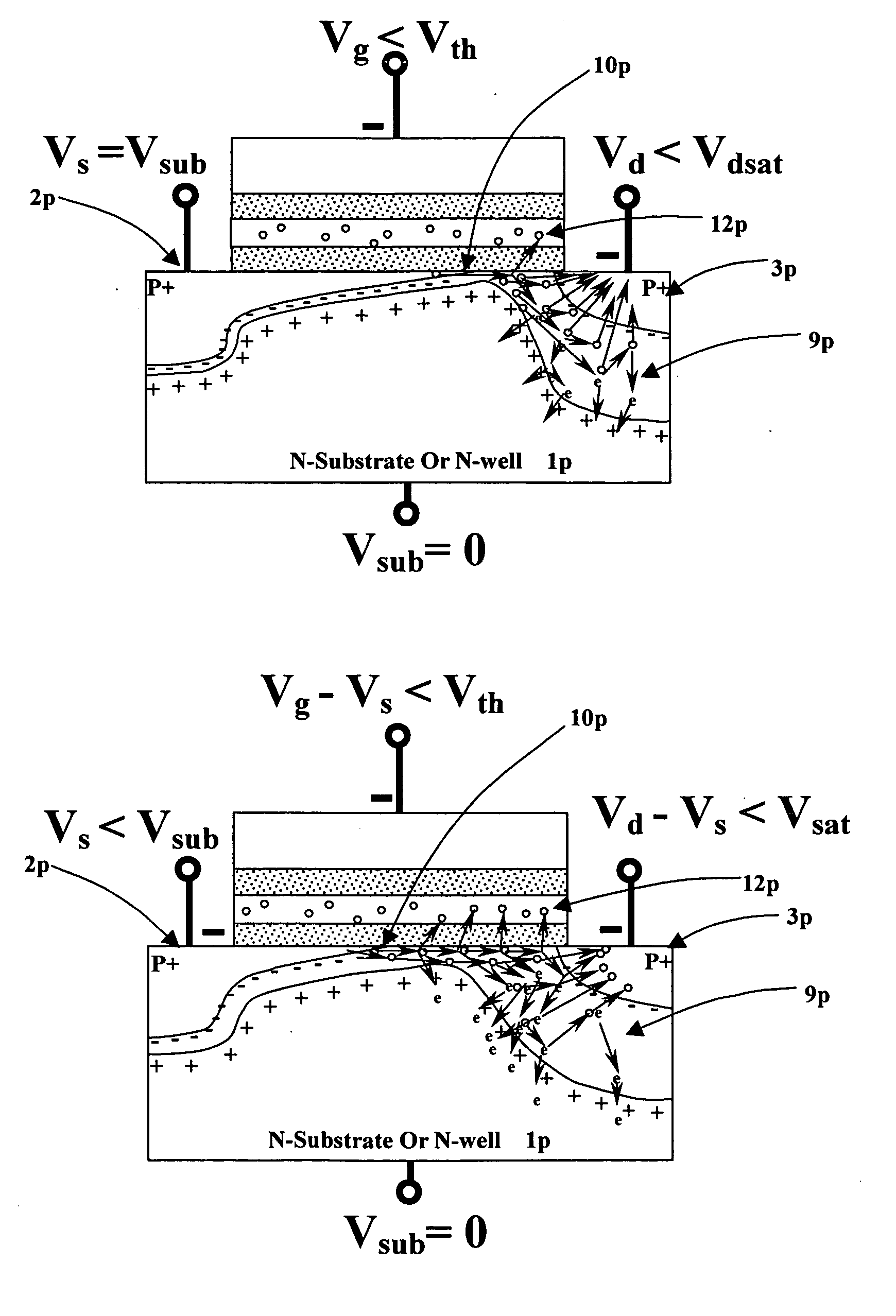
[0013] The advantage of the present invention is to provide a low-programming voltage scheme with the features those can relieve the loading for charge pumping circuit and programming disturbance in EEPROMs. It allows designing a smaller charge pumping circuit and increasing EEPROM cell density. For EEPROM erasing scheme, the self-convergent low-voltage erasing can achieve very narrow distributions for the device electrical properties after the erase operations. A convergent circuit is not required in this erasing scheme. The present invention scheme can dramatically improve the NVM cost in terms of densities, sizes, and power. The aspects of the present invention are briefly described as follows.
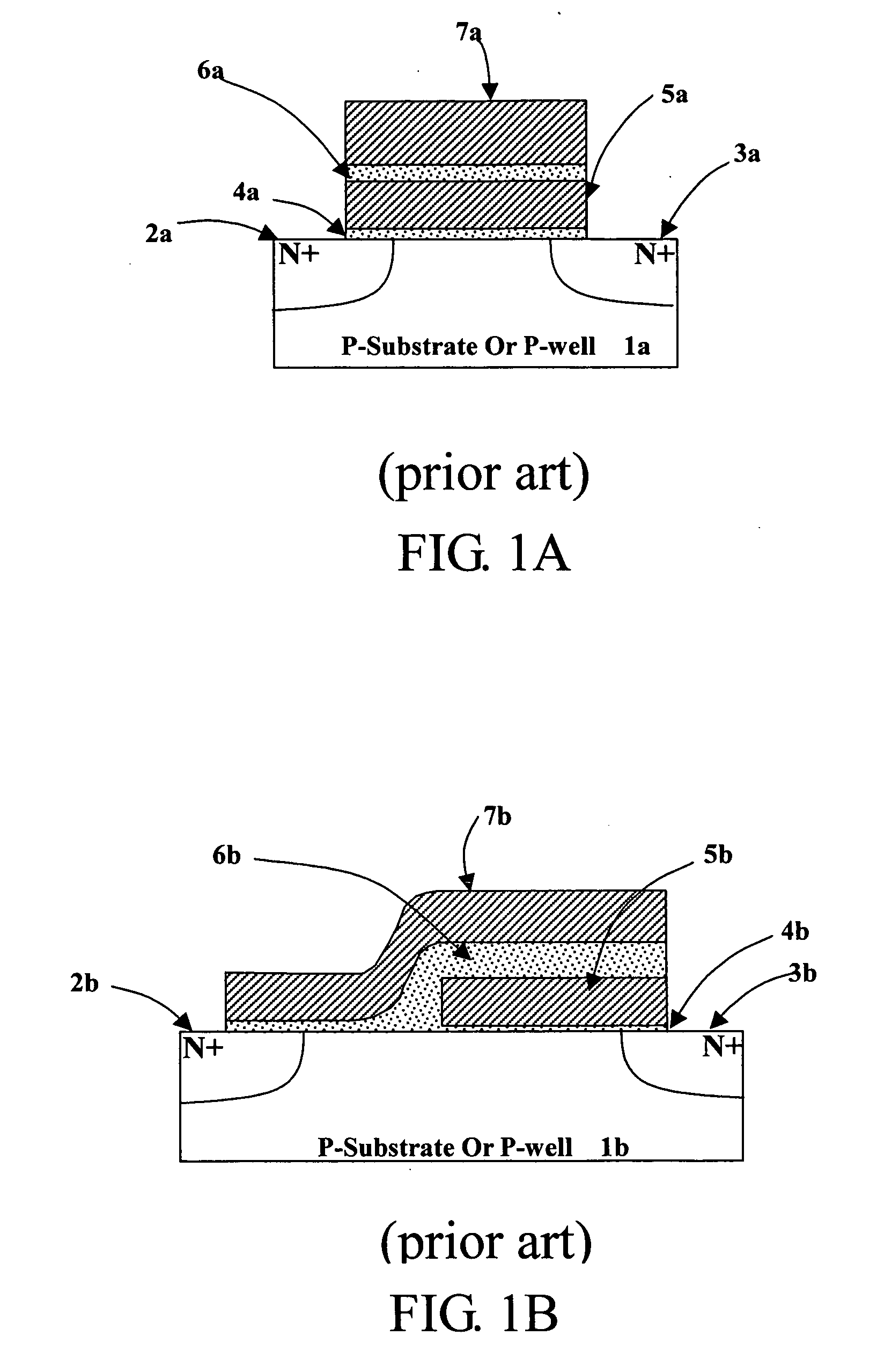
[0014] The present invention discloses a method of programming a NFET based nonvolatile memory, comprising: applying on a source a positive source voltage relative to a substrate to create a reversed-bias voltage on a source-substrate junction; and applying a first and a second positive voltages to a control gate and a drain, respectively.
[0015] The difference between the first positive voltage and the positive source voltage is greater than the threshold voltage of the nonvolatile memory. The second positive voltage greater than the source voltage is sufficient large to cause DAHCI in the drain depleted region. The Programming Scheme for PFET Based Nonvolatile Memory:
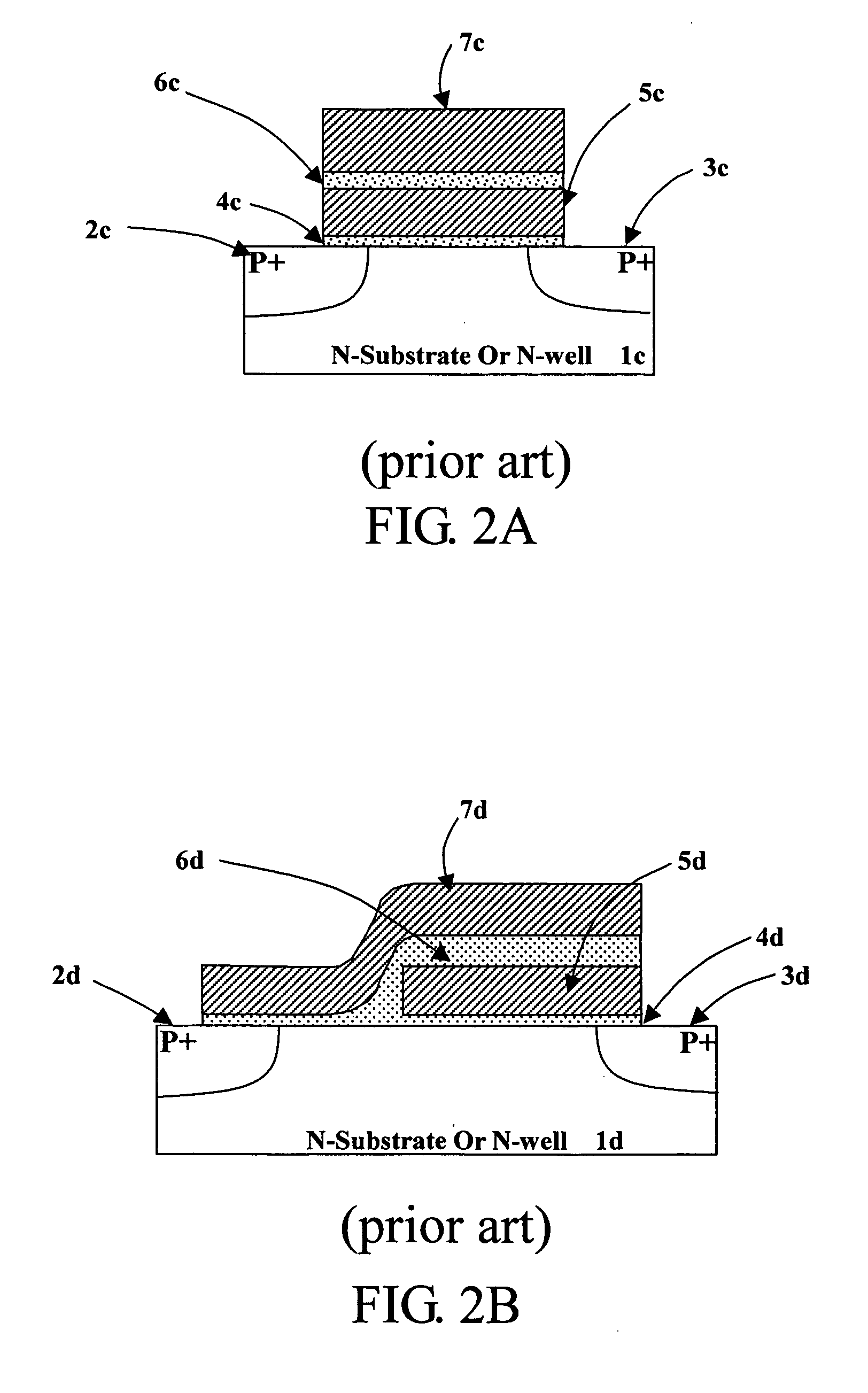
[0016] Another aspect of the present invention is to provide a method of programming a PFET based nonvolatile memory comprising: assuming the substrate or Nwell is grounded; applying on a source a negative source voltage relative to a substrate to create a reversed-bias voltage on a source substrate junction; and applying the first and second negative voltages to a control gate and a drain, respectively.
[0017] In the scheme, the absolute value of the difference between the first negative voltage and the negative source voltage is greater than the one of the threshold voltage of the nonvolatile memory. The absolute value of the difference between the second negative voltage and the negative source voltage is sufficient large to cause DAHCI in the drain depleted region.
[0018] Further embodiments of programming bias schematics of the preferred embodiments for NFET and PFET are provided. It shall be noted that both NFET and NFET can be implemented with only one high positive voltage Vddh without switching to negative voltages for PFET. The Erasing Scheme for NFET Based Nonvolatile Memory:

Problems solved by technology

Thus, the programming efficiency using the conventional DAHCI is very low.
The other side effect of this higher voltage and higher current operation is that the disturbance to the neighbor cells through the substrate becomes more significant, especially for higher density EEPROM.
Those advert effects limit the EEPROM design for higher density leading to lower cost.
The main issues with the FNT erase are the widely disperse distribution after erase operations and the requirement for very high voltages (about 12 V for a typical oxide thickness).
When high voltage is applied to cause tunneling between floating gate and the substrate, microscopically, the tunneling current is not uniform across the source, drain, junction depletion, and channel regions.
The applied voltage difference will cause variations of electrical fields in source, drain, and junction depletion regions resulting in variations of total tunneling currents.
However, this approach not only needs more silicon area for the convergent circuit but also requires a lengthy and time-consuming operation procedure.

Method used


Image

  • High-speed low-voltage programming and self-convergent high-speed low-voltage erasing schemes for EEPROM
  • High-speed low-voltage programming and self-convergent high-speed low-voltage erasing schemes for EEPROM
  • High-speed low-voltage programming and self-convergent high-speed low-voltage erasing schemes for EEPROM

Examples


Embodiment Construction

[0040] Method and structure for manufacturing a semiconductor device (such as integrated circuit) or a substrate is described below. In the following description, numerous specific details are set forth in order to provide a thorough understanding of the present invention, and the scope of the present invention is expressly not limited expect as specified in the accompanying claims. One skilled in the relevant art will recognize, however, that the invention may be practiced without one or more of the specific details. In other instances, well known structures, materials, or operations are not shown or described in order to avoid obscuring aspects of the invention.

[0041] The present invention includes methods and schematics to achieve high-speed low-voltage programming and self-convergent high-speed low-voltage Erasing for Electrically Erasable Programmable Read-Only Memory (EEPROM). Those of ordinary skill in the art will immediately realize that the embodiments of the present inve...


PUM


Abstract

The present invention provides a high-speed low-voltage programming scheme and self-convergent high-speed low-voltage erasing schemes for Electrically Erasable Programmable Read-Only Memories (EEPROM). For the N-type Field Effect Transistor (NFET) based NVM programming, an elevated source voltage to the substrate can achieve high efficient Drain-Avalanche-Hot-Electron Injection (DAHEI) into the floating gate resulting in high-speed and low-voltage operations. The self-convergent and low-voltage erasing can be achieved by applying Drain-Avalanche-Hot Hole Injection (DAHHI) with the conditions of restricted maximum drain current and a moderate control gate voltage enough to turn on the NFET. For the p-type FET (PFET) based EEPROM programming, a negative source voltage relative to the substrate can achieve high efficient Drain-Avalanche-Hot-Hole Injection (DAHHI) into the floating gate resulting in high-speed and low voltage operations. The self-convergent and low voltage erasing can be achieved by applying Drain-Avalanche-Hot-Electron Injection (DAHEI) with the conditions of restricted maximum magnitude of drain current and a negative moderate control gate voltage enough to turn on the PFET.

Description

BACKGROUND OF THE INVENTION [0001] 1. Field of the Invention [0002] This invention relates to Electrically Erasable, Programmable Read-Only Memories (EEPROM), and more particularly, to a programming and erasing schemes for EEPROM to enable high-speed low-voltage programming operations and self-convergent high speed low-voltage erasing operations. [0003] 2. Description of the Prior Art [0004] Electrically Erasable PROMs depend on the long-term retention of electronic charges as the information-storage mechanism. The charges are stored on a floating polysilicon gate of a MOS device (the term floating refers to the fact that no electrical connection exists to this gate). The charges are transferred from the silicon substrate through an insulator. [0005] Semiconductor Non-Volatile Memories (NVM), and particularly Electrically Erasable, Programmable Read-Only Memories (EEPROM), exhibit wide spread applicability in a range of electronic equipments from computers, to telecommunications har...

Claims


Application Information

Patent Timeline
IPC IPC(8): H01L29/788
CPCG11C16/0416H01L29/7885G11C16/14G11C16/10
Inventor HUANG, DANIELWANG, LEELIN, HSIN CHANGCHANG, ROGET
Owner YIELD MICROELECTRONICS CORP
Learn More