Peel strength simulating apparatus, peel strength simulating program storage medium, and peel strength simulating method

a technology of peel strength and simulating program, applied in the field of peel strength simulating program storage medium, peel strength simulating method, can solve the problems of increased production cost, increased cost of semiconductor integrated circuit device, increased production cost, etc., and achieves high reliability, peel strength, and suppressed cost increase

Inactive Publication Date: 2007-06-21
FUJITSU LTD
View PDF4 Cites 0 Cited by
  • Summary
  • Abstract
  • Description
  • Claims
  • Application Information

AI Technical Summary

Benefits of technology

[0011] The present invention has been made in view of the above circumstances and provides a peel strength simulating apparatus, a peel strength simulating program storage medium, and a peel strength simulating method in which the highly-reliable semiconductor integrated circuit device can be obtained by sufficiently enhancing peel strength between the semiconductor integrated circuit chip and resin package bonded to each other while the cost increase is suppressed.
[0017] The peel strength simulating apparatus of the invention is an apparatus in which the changeable conditions (numerical values), changeable conditions (group of numerical values), and the change priorities are specified, and the simulating section repeats the simulation of the peel strength until the peel strength exceeding the predetermined threshold value is obtained while simulating section changes the specified conditions according to the specified priorities. Therefore, the peel strength simulating apparatus of the invention can provide the semiconductor integrated circuit device having the peel strength matching the production condition and the usage condition of the semiconductor integrated circuit device between the semiconductor integrated circuit chip and the resin package, which allows the cost increase to be suppressed.
[0024] The peel strength simulating program storage medium of the invention is executed in the peel strength simulating apparatus which simulates the peel strength between the semiconductor integrated circuit chip and the resin package bonded to each other. Therefore, the peel strength simulating program storage medium of the invention can provide the highly-reliable semiconductor integrated circuit device in which the peel strength between the semiconductor integrated circuit chip and the resin package bonded to each other is sufficiently enhanced while the cost increase is suppressed.
[0029] The peel strength simulating method of the invention is a method in which the changeable conditions (numerical values), changeable conditions (group of numerical values), and the change priorities are specified, and the simulation of the peel strength is repeated until the peel strength exceeding the predetermined threshold value is obtained while the specified conditions are changed according to the specified priorities. Therefore, in producing the semiconductor integrated circuit device, the semiconductor integrated circuit device having the peel strength matching the production condition and the usage condition of the semiconductor integrated circuit device between the semiconductor integrated circuit chip and the resin package can be produced while the cost increase is suppressed.
[0030] Accordingly, the present invention can provide a peel strength simulating apparatus, a peel strength simulating program, and a peel strength simulating method in which the highly-reliable semiconductor integrated circuit device can be obtained by sufficiently enhancing peel strength between the semiconductor integrated circuit chip and resin package bonded to each other while the cost increase is suppressed.

Problems solved by technology

When an excessive load due to temperature variation or a mechanical load is applied, sometimes there is generated a problem that the semiconductor integrated circuit chip and the resin package are peeled off each other at the boundary between the semiconductor integrated circuit chip and the resin package.
In this case, when the under fill material is not sufficiently charged, there is a fear that the peel is generated at the boundary between the semiconductor integrated circuit chip and the resin package after a reflow process, so that it is necessary to sufficiently manage a process of charging the under fill material.
This causes a problem that production cost is increased.
For the case where the U-shaped groove is made in the lower surface of the semiconductor integrated circuit chip, when the U-shaped groove made is not large enough, there is the fear that the peel is generated at the boundary between the semiconductor integrated circuit chip and the resin package, so that it is necessary to sufficiently manage a process of making the size of the under fill material.
This also causes the problem that the production cost is increased.
Accordingly, there is the problem that the cost is increased in the semiconductor integrated circuit device.

Method used


Image

  • Peel strength simulating apparatus, peel strength simulating program storage medium, and peel strength simulating method
  • Peel strength simulating apparatus, peel strength simulating program storage medium, and peel strength simulating method
  • Peel strength simulating apparatus, peel strength simulating program storage medium, and peel strength simulating method

Examples


Embodiment Construction

[0042] Preferred embodiments of the invention will be described below.

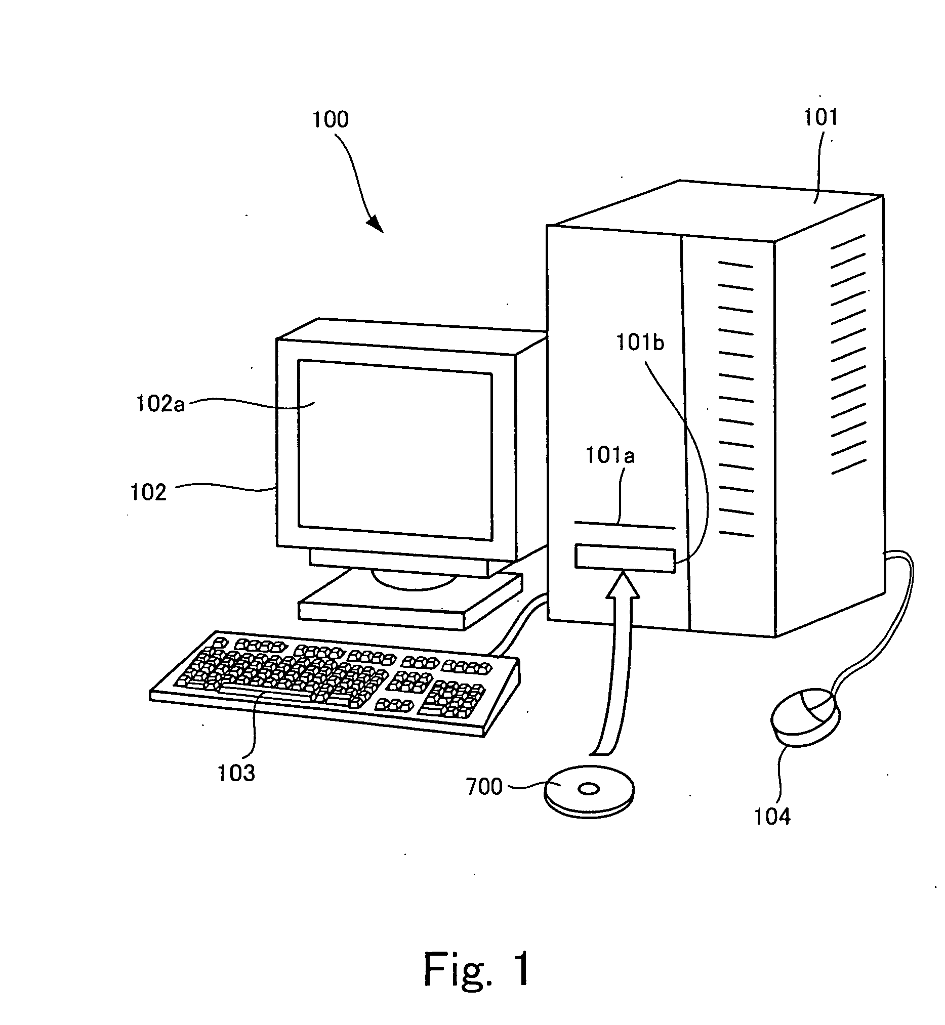
[0043]FIG. 1 is a schematic view showing an information processing apparatus in which a peel strength simulating apparatus according to an embodiment of the invention is realized.

[0044]FIG. 1 shows a computer 100 generally called a workstation or a personal computer which is of the information processing apparatus, and the computer 100 realizes a peel strength simulating apparatus according to the embodiment of the invention. A peel strength simulating method according to an embodiment of the invention is applied to the peel strength simulating apparatus of the embodiment. A hardware configuration of the computer 100 will be described.

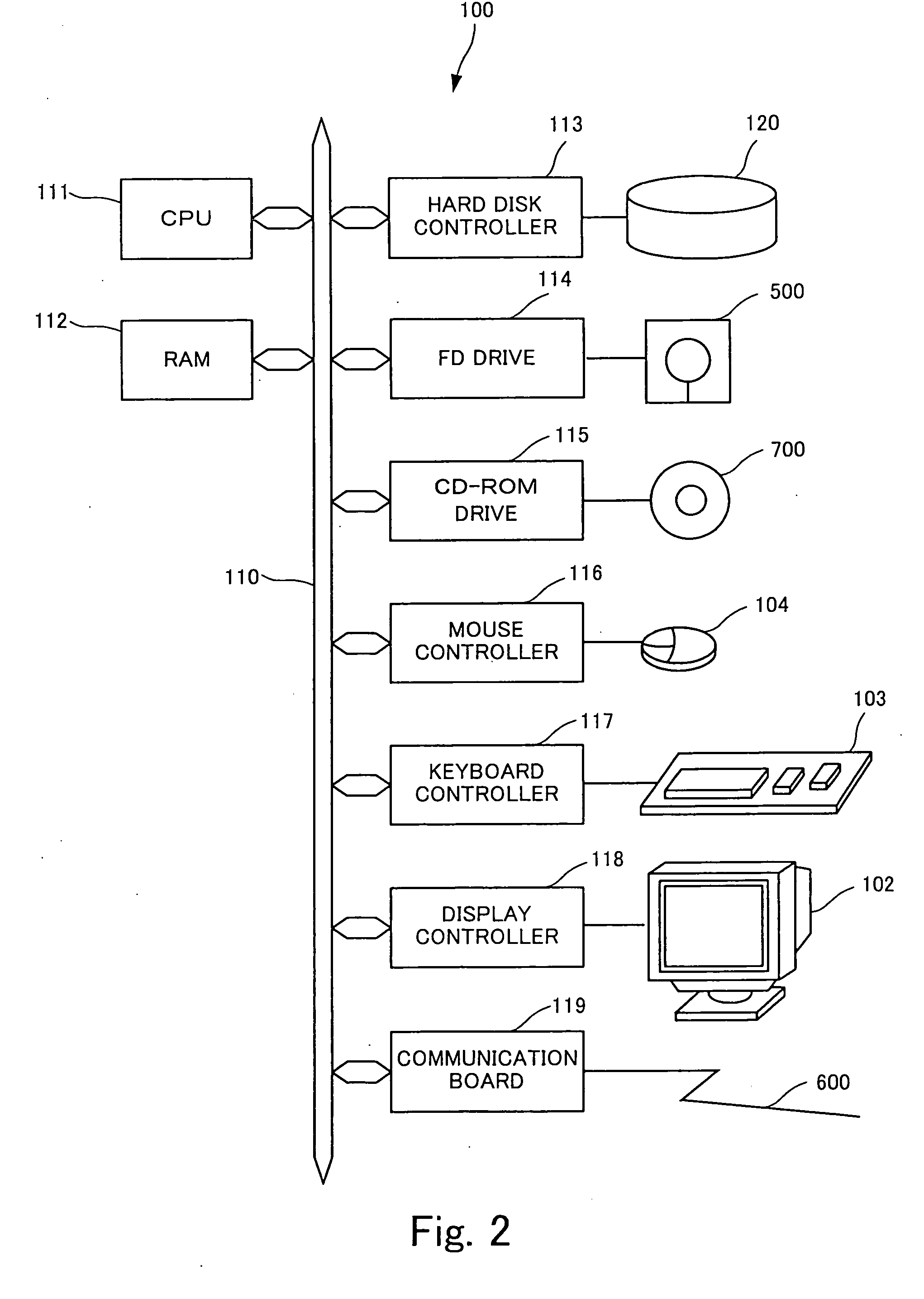
[0045] The computer 100 includes a main body section 101, a display section 102, a keyboard 103, and a mouse 104. CPU (Central Processing Unit), RAM (Random Access Memory), a hard disk, a communication board, and the like are incorporated in the main body section 101. The display ...


PUM


Abstract

The present invention provides a peel strength simulating apparatus which simulates peel strength between a semiconductor integrated circuit chip and a resin package bonded to each other. The apparatus includes a storage section which stores plural types of parameters. The apparatus also includes a parameter specifying section which specifies a changeable parameter whose numerical value is changeable from the plural types of parameters stored in the storage section and specifies change priorities when specifying plural types of changeable parameters. The apparatus further includes a simulating section which repeats simulation of the peel strength until the peel strength exceeding a predetermined threshold value is obtained while changing the numerical values of the specified changeable parameters according to the specified priorities.

Description

BACKGROUND OF THE INVENTION [0001] 1. Field of the Invention [0002] The present invention relates to a peel strength simulating apparatus for simulating peel strength between a semiconductor integrated circuit chip and a resin package which are bonded to each other, a peel strength simulating program storage medium in which a peel strength simulating program running on the peel strength simulating apparatus is stored, and a peel strength simulating method. [0003] 2. Description of the Related Art [0004] Recently, as physical sizes of electronic instruments are reduced, physical sizes of semiconductor integrated circuit devices mounted on the electronic instruments are also reduced more and more. In such semiconductor integrated circuit devices, there is known a semiconductor integrated circuit device in which SCSP (Super Chip Size Package) having the size extremely close to the size of a semiconductor integrated circuit chip (silicon chip) is adopted. The SCSP type semiconductor int...

Claims


Application Information

Patent Timeline
Patent Type & Authority Applications(United States)
IPC IPC(8): H01L23/48
CPCG06F17/5018G06F2217/40H01L24/13H01L24/16H01L2224/1308H01L2224/13082H01L2224/131H01L2224/13147H01L2224/83102H01L2224/92125H01L2924/01029H01L2924/14H01L2924/00014H01L2924/014H01L2924/00013H01L2924/01005H01L2924/01006H01L2924/01033H01L2924/01047H01L2224/13099H01L2924/10253H01L2924/00G06F30/23G06F2113/18H01L2224/05573H01L2224/05647H01L2924/351
Inventor NAKADATE, MAMI
Owner FUJITSU LTD
Why Eureka
Try Eureka