Magnetoresistive element and magnetic memory device
- Summary
- Abstract
- Description
- Claims
- Application Information
AI Technical Summary
Benefits of technology
Problems solved by technology
Method used
Image
Examples
first embodiment
(First Embodiment)
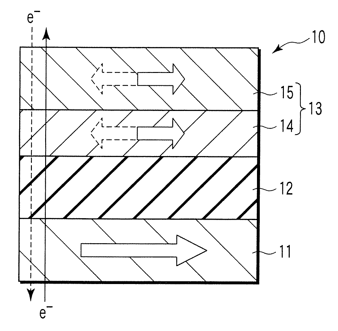
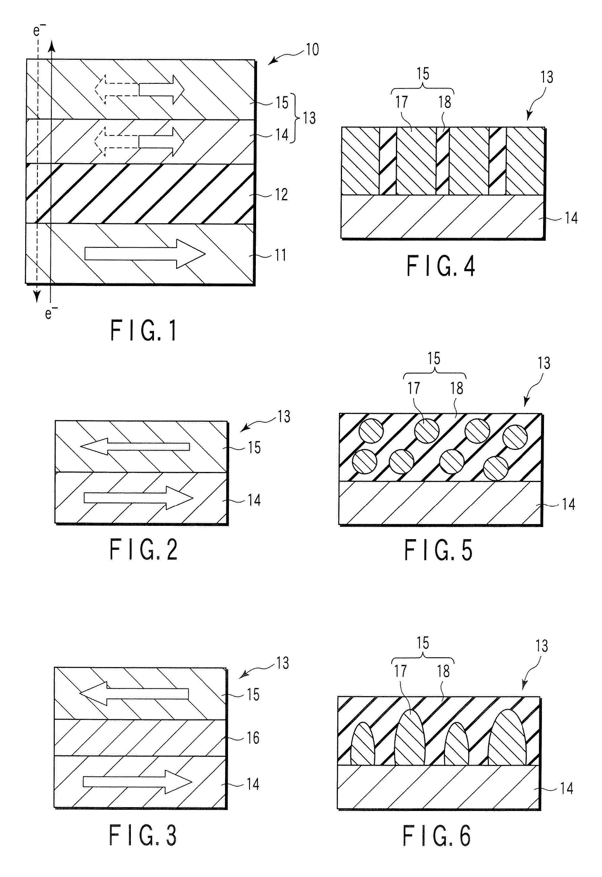
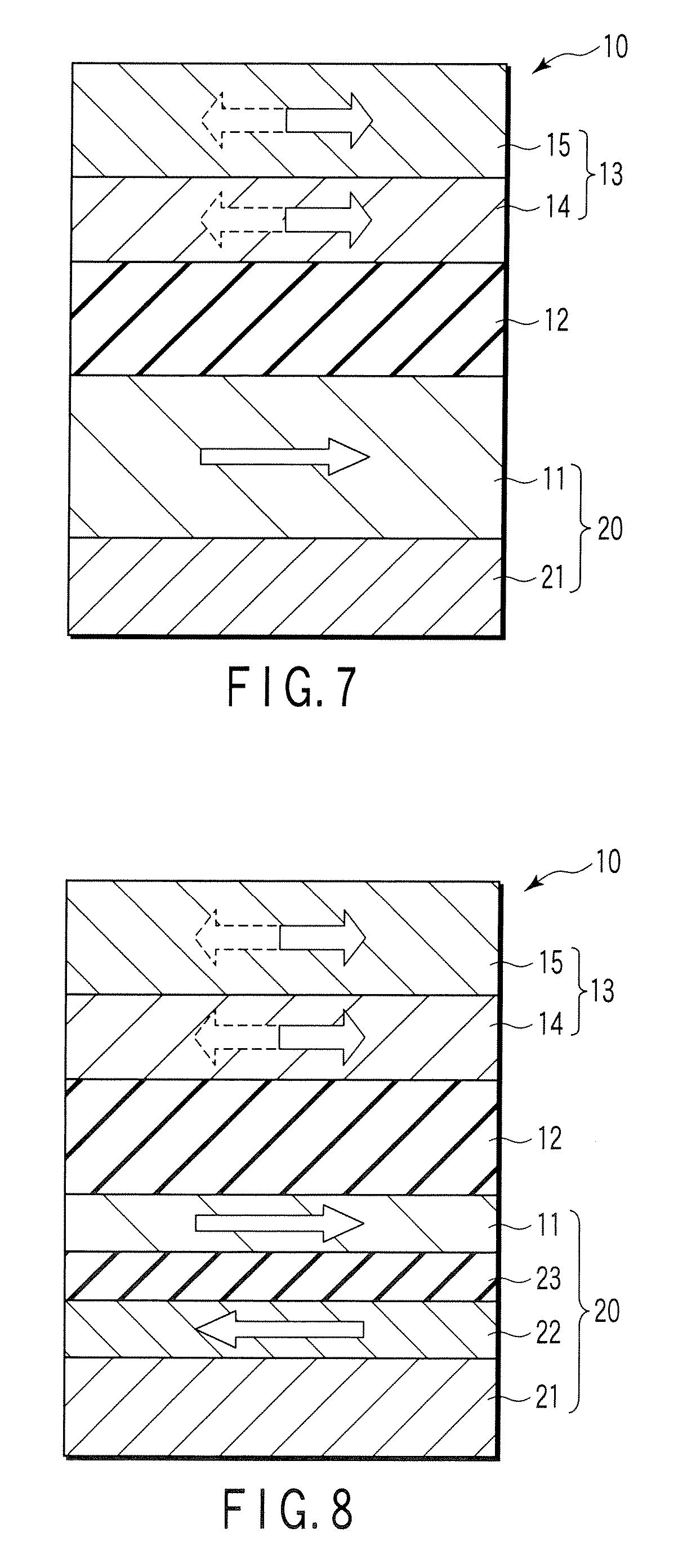
[0032]FIG. 1 illustrates the magnetoresistive element (MR element) 10 having, e.g., planar magnetization alignment. Each arrow in the drawings indicates a magnetization direction.
[0033] This embodiment uses spin momentum transfer. A bidirectional current in the out-of-plane direction (in the direction perpendicular to the plane) is supplied to the MR element 10 to switch the magnetization of a magnetic recording layer by the function of spin of electrons. That is, the MR element 10 is a spin transfer magnetoresistive element capable of switching magnetization by supplying spin-polarized electrons (spin injection).
[0034] The MR element 10 includes a magnetic recording layer (free layer) 13 having a laminated structure of an interface magnetic layer 14 and magnetic stabilizing layer 15, a magnetic reference layer (pinned layer) 11, and a nonmagnetic layer 12 sandwiched between the magnetic recording layer 13 and the magnetic reference layer 11. The magnetization di...
examples
[0121] A plurality of examples of the MR element 10 will be described below. First, the size and manufacturing method of the MR element 10 used as examples will be described.
[0122] An MR element 10 is formed between a lower electrode layer and an upper electrode layer. More specifically, an MTJ film is formed on the lower electrode layer by, e.g., DC magnetron sputtering. The lower electrode layer uses, e.g., Ta. The MTJ film is patterned to a size of about 0.1×0.15 μm2 by photolithography using an excimer laser. At this time, a magnetic recording layer 13 has an aspect ratio (long axis / short axis) of 1.5. Then, the MR element 10 is fabricated by ion beam etching (IBE).
[0123] An interlayer insulating layer is formed next. The interlayer insulating layer is planarized by chemical mechanical polishing (CMP) to expose the upper surface of the MR element 10. An upper electrode layer is formed on the MR element 10. The upper electrode layer uses, e.g., Ta. Barrier formation conditions ...
PUM
 Abstract
Description
Claims
Application Information
 - R&D
- Intellectual Property
- Life Sciences
- Materials
- Tech Scout
- Unparalleled Data Quality
- Higher Quality Content
- 60% Fewer Hallucinations
Browse by: Latest US Patents, China's latest patents, Technical Efficacy Thesaurus, Application Domain, Technology Topic, Popular Technical Reports.
© 2025 PatSnap. All rights reserved.Legal|Privacy policy|Modern Slavery Act Transparency Statement|Sitemap|About US| Contact US: help@patsnap.com


