Thermal expansion compensation graded IC package

a technology of thermal expansion compensation and ic package, which is applied in the direction of printed circuit stress/warp reduction, printed circuit aspects, printed circuit manufacturing, etc., can solve the problems of thermal expansion difference between the semiconductor device and the circuit board, increase the clock speed, and increase the number of inputs and outputs, so as to achieve the effect of reducing stress

Inactive Publication Date: 2007-04-12
SUN MICROSYSTEMS INC
View PDF20 Cites 19 Cited by
  • Summary
  • Abstract
  • Description
  • Claims
  • Application Information

AI Technical Summary

Benefits of technology

[0020] In accordance with the present invention, an approach for incrementally and / or locally mitigating the stresses imposed when bonding two or more substrates with different thermal expansion characteristics is set forth which incrementally and / or locally compensates for the thermal expansion differences between a semiconductor die and package by the insertion of a plurality of intermediate compensator devices between the die, other devices, and the package. The compensator devices can be physically connected on either side to the package, another compensator device, other devices, or the die, as needed through solder bump attach, or some equivalent method. The approach provides electrical connection and thermal dissipation between the die and package as well as providing mechanical protection for the die bumps and internal die structures by absorbing the stresses imposed by the thermal expansion differences.

Problems solved by technology

Integrated circuit technology continues to evolve, resulting in chips with increased clock speeds, higher power consumption, and larger numbers of inputs and outputs.
A fundamental issue in semiconductor package mounting is the thermal expansion differences between the semiconductor device and the circuit board.
Mechanical protection of the semiconductor device can be jeopardized if thermal mismatches between the device, package and / or circuit board are not sufficiently accommodated.
These stresses can produce failures within the components themselves or at any of the interfaces between components.
The flip-chip method of device-to-package attachment is especially sensitive to this issue.
The most severe stress is due to the inherently large thermal coefficient of expansion mismatch between the plastics and the metals commonly used in fabrication techniques.
These stresses produce instantaneous elastic and plastic strains, particularly at the weakest interconnection structure, which causes shear displacements that can fracture solder ball connections.
Over its lifetime, the functionality of the electronic package will be destroyed if the flip chip and / or substrate are unable to repeatedly bear their respective share of thermal mismatch.
As the device size grows, the issue can become more pronounced, resulting in the dilemma of whether package thermal expansion should be matched to the device or the circuit board.
Sockets present significant cost versus performance trade-offs.
A socket that represents a marginal material cost increase can result in significant electrical performance degradation.
Further, such sockets may require pins to be placed on the package, adding process steps and cost, thereby offsetting potential savings.
Conversely, a socket that does not degrade performance or require pins can cost as much as the package itself.
In addition, such sockets can require significant force be placed on the package to ensure good socket contact, which limits mechanical and thermal design solutions.
Additionally, sockets or interposers can degrade the reliability of the package.
They provide proper stand-off and ensure good electrical connection, but they are difficult to process and currently limited in the supplier base.
However, this method adds complications and associated costs to the assembly process.
Interposers are yet another solution, but currently this solution is relatively untested and inherently undesirable, as they can result in higher material costs, additional processing costs during assembly, and they do not allow interconnection routing.
Unfortunately, as the device grows larger, even the underfill cannot reduce inherent stresses to non-fatal levels, and if used alone, could require significant process and material development to become a viable solution for large dies.
Unfortunately, a dielectric material's strength seems to be directly proportional to its K value, causing the dielectric material to become more susceptible to stress as its K value decreases.
Current trends in semiconductor design to aggressively increase circuit density, with a corresponding reduction in die sizes, can result in increased heat dissipation, which in turn can exacerbate coefficient of thermal expansion (CTE) mismatch between package components.
This can result in a decrease in the bump pitch for a flip-chip, which often means increasing the number of connections to support the additional power required for increased performance.
The combined effect of reduced bump pitch and increased power connectors further affects CTE mismatch.
However, while the CTE of organic packaging is more closely matched to that of the circuit board than ceramic, it may be insufficient to accommodate certain CTE mismatch situations.
For example, clustering of high power units can lead to localized concentrations of higher heat flux, manifested as large temperature gradients across the surface of the die, whose variations may be too great to be accommodated by the CTE of an organic package.
Similarly, the CTE characteristics of a given organic package may not be able to accommodate the aggregate CTE of individual components comprising a composite semiconductor assembly.

Method used


Image

  • Thermal expansion compensation graded IC package
  • Thermal expansion compensation graded IC package
  • Thermal expansion compensation graded IC package

Examples


Embodiment Construction

[0037] Although the present invention has been described in detail, it should be understood that various changes, substitutions and alterations can be made hereto without departing from the spirit and scope of the invention as defined by the appended claims.

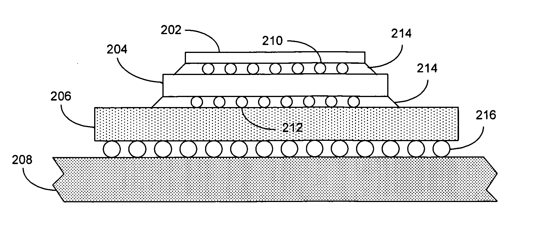
[0038]FIG. 1 shows a computer system 100 in accordance with an embodiment of the present invention. As illustrated in FIG. 1, computer system 100 includes processor 102, which is coupled to a memory 112 and to peripheral bus 110 through bridge 106. Bridge 106 can generally include any type of circuitry for coupling components of computer system 100 together.

[0039] Processor 102 can include any type of processor, including, but not limited to, a microprocessor, a mainframe computer, a digital signal processor, a personal organizer, a device controller and a computational engine within an appliance. Processor 102 includes a cache 104 that stores code and data for execution by processor 102.

[0040] Processor 102 communicates with ...


PUM


Abstract

An apparatus and method for connecting one substrate, such as a semiconductor die, to an opposing substrate, such as a semiconductor package or circuit board, through a plurality of intermediate thermal compensator devices, each of which can incrementally and/or locally mitigate the stresses imposed by differences in the two substrate's thermal expansion characteristics. The compensator devices can be coupled to one another, with the resulting assembly attached to the first substrate on one side, and to the second substrate on the other side, through solder bump attach, or some equivalent method. The method of the invention provides electrical connection and thermal dissipation between the two substrates as well as providing mechanical protection by absorbing the stresses imposed by the difference in thermal expansion characteristics of the two substrates.

Description

BACKGROUND OF THE INVENTION [0001] 1. Field of the Invention [0002] The present invention relates to packaging integrated circuits, and more specifically, to mitigating the stresses imposed when bonding two or more substrates with different thermal expansion characteristics. [0003] 2. Description of the Related Art [0004] Integrated circuit technology continues to evolve, resulting in chips with increased clock speeds, higher power consumption, and larger numbers of inputs and outputs. Corresponding advances in integrated circuit fabrication technology have resulted in higher levels of integration, increased density, and growth in die sizes. [0005] A semiconductor device is an integrated circuit in packaged form, usually mounted to printed circuit boards (“circuit boards”) or other type of carrier, operating as a processing unit, memory, controller or any other electronic device. Semiconductor package and packaging techniques are designed to provide electrical connection between the...

Claims


Application Information

Patent Timeline
Patent Type & Authority Applications(United States)
IPC IPC(8): H01L23/02
CPCH01L23/50H01L2224/16225H01L25/0657H01L2224/32145H01L2224/83102H01L2224/92125H01L2225/06513H01L2225/06517H01L2225/06589H01L2924/09701H01L2924/15311H01L2924/19105H01L2924/3011H05K1/0271H05K1/141H05K3/3436H05K2201/049H05K2201/068H05K2201/10734H05K2201/10977H01L2924/01019H01L2224/16265H01L23/5385
Inventor KIRKMAN, SCOTTSEN, BIDYUT
Owner SUN MICROSYSTEMS INC
Why Eureka
Try Eureka