
Resist pattern thickening material and process for forming resist pattern, and semiconductor device and process for manufacturing the same

a technology of resist pattern and thickening material, which is applied in the direction of photosensitive materials, instruments, photomechanical equipment, etc., can solve the problems of difficult development of new resist materials suitable for exposure light with short wavelengths, difficult control of thickening amount, and difficulty in improving exposure devices. , to achieve the effect of good thickening effect, easy control of thickening amount, and easy and precise formation

Inactive Publication Date: 2007-03-01
FUJITSU LTD
View PDF7 Cites 17 Cited by
  • Summary
  • Abstract
  • Description
  • Claims
  • Application Information

AI Technical Summary

Benefits of technology

[0015] In view of the above-mentioned problems, inventors of the present invention have investigated vigorously and have obtained the following knowledge. Specifically, when a resist pattern is swelled using a conventional resist swelling material, because it relies on crosslinking reaction accelerated by an acid or its diffusion, the swelling amount (thickening amount) is altered greatly by the thickening conditions of temperature, density difference of pattern, or the like. However, it was found that when a solubilizer which melts the resist pattern at the temperature near its melting point and water-soluble element are used as a resist pattern thickening material, the thickening amount of resist pattern can be easily controlled regardless of thickening conditions because no crosslinking reaction by an acid is used.
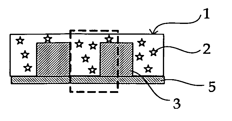
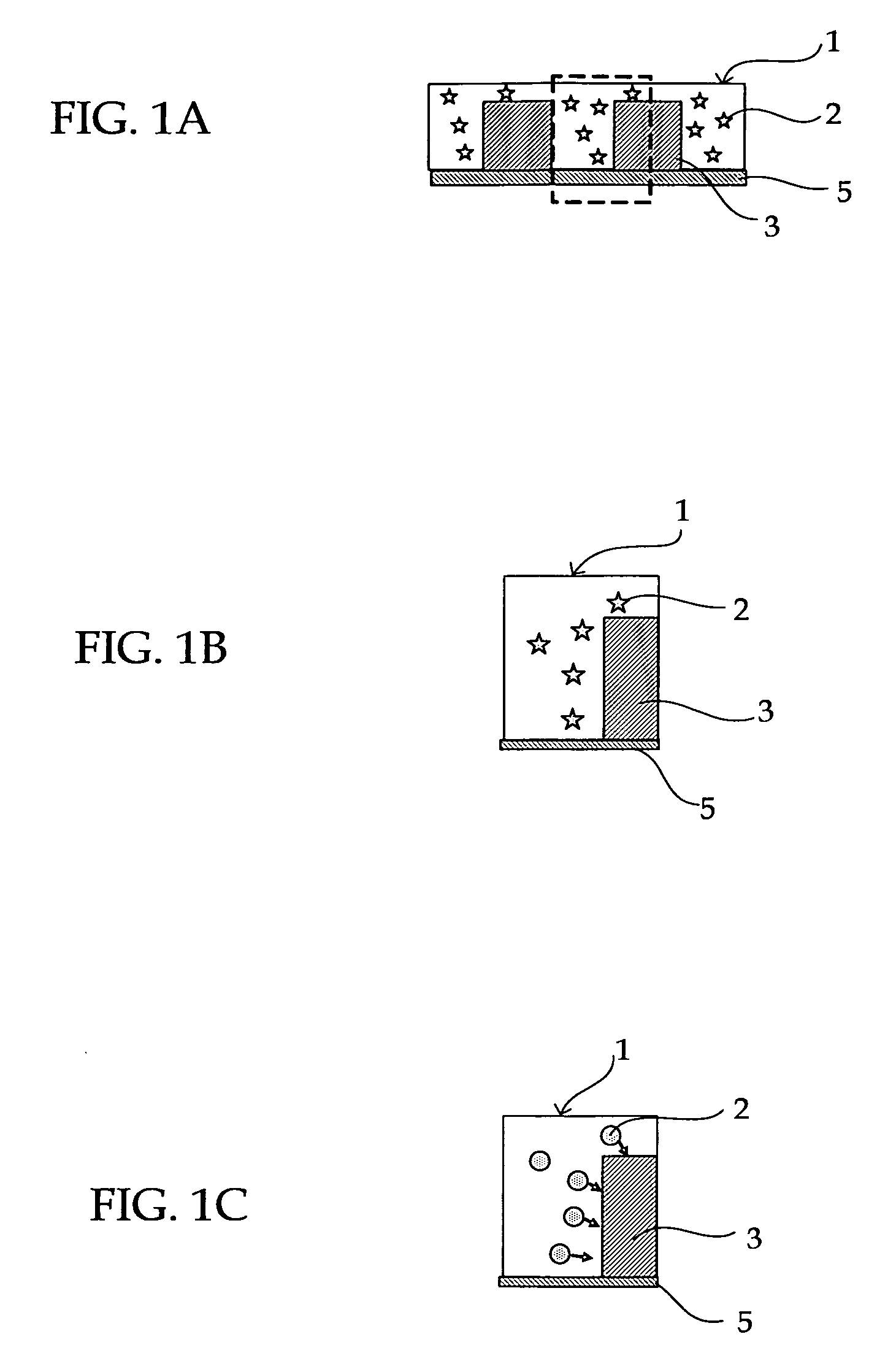
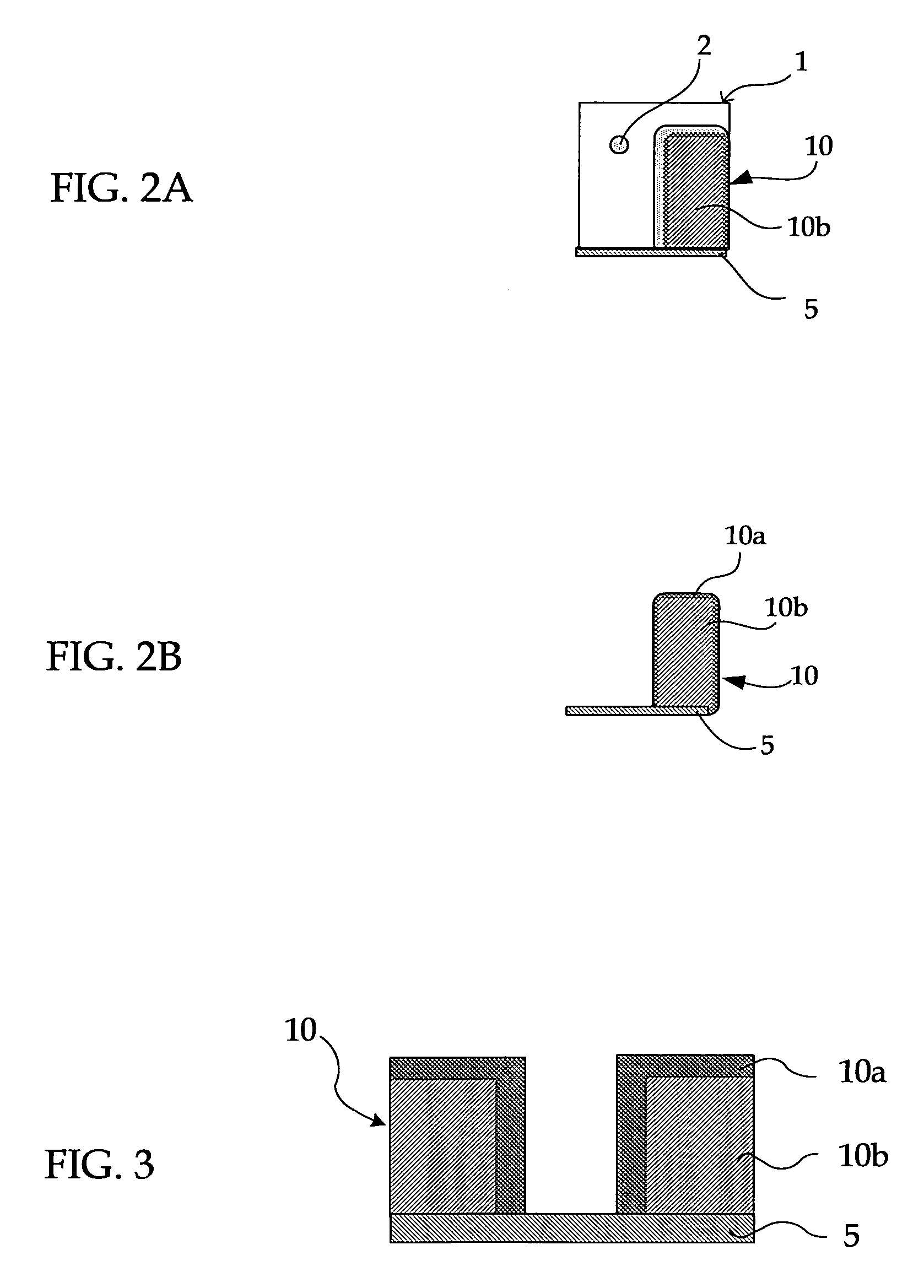
[0018] In the resist pattern thickening material, a solubilizer which melts the resist pattern at the temperature near its melting point (hereafter may be referred to as “solubilizer”) is dispersed in water-soluble element and when the resist pattern thickening material is coated on the resist pattern and heated at near the melting point of the solubilizer, the solubilizer becomes fused. Then the material of the resist pattern is melted by fused solubilizer and the water-soluble element, solubilizer and the material of the resist pattern interact (are mixed) with each other. At this time, a surface layer (mixing layer), where the resist pattern thickening material and the resist pattern are mixed, is efficiently formed on the surface of the resist pattern which becomes an inner layer. As a result, the resist pattern is efficiently thickened (hereafter may be referred to as “swelling”) by the resist pattern thickening material. The resist pattern thickened in this way (hereinafter may be referred to as “thickened resist pattern”) is thickened uniformly by the resist pattern thickening material. Thus, a space pattern formed by the thickened resist pattern has a fine structure beyond the exposure or resolution limits. The term “space pattern” is hereby defined as a hole, trench, recess, or any other empty space that is formed by developing a resist. Since the resist pattern thickening material of the present invention contains a solubilizer which melts the resist pattern at the temperature near its melting point and a water-soluble element and does not contain crosslinkable element, therefore, no crosslinking reaction is induced by acid and a good thickening effect can be obtained regardless of thickening conditions such as temperature, density difference of pattern, etc. and the thickening amount of the resist pattern can be easily controlled to form a desired space pattern. Thus, the resist pattern thickening material of the present invention can be suitably utilized for forming a resist pattern such as lines and spaces pattern, etc. used for wiring layer of LOGIC LSI where resist patterns of various sizes are mixed.
[0019] The process for forming a resist pattern of the present invention includes forming a resist pattern, and then coating a resist pattern thickening material of the present invention over the surface of the resist pattern. In the process for forming a resist pattern of the present invention, a resist pattern is formed and when the resist pattern thickening material is coated over the resist pattern and heated at near the melting point of the solubilizer, the solubilizer within the resist pattern thickening material, which are dispersed in water-soluble element and melts the resist pattern at the temperature near its melting point, is fused. Then the material of the resist pattern is melted by fused solubilizer and the water-soluble element, the solubilizer and the material of the resist pattern interact (are mixed) with each other. Thus, a surface layer (mixing layer), where the resist pattern thickening material and the resist pattern are mixed, is formed on the surface of the resist pattern which becomes an inner layer. The resulting thickened resist pattern is uniformly thickened by the resist pattern thickening material. Thus, the space pattern formed by the thickened resist pattern has a fine structure beyond the exposure or resolution limits. Since the resist pattern thickening material of the present invention contains a solubilizer which melts the resist pattern at the temperature near its melting point and a water-soluble element and does not contain crosslinkable element, therefore, no crosslinking reaction is induced by an acid and a good thickening effect can be obtained regardless of thickening conditions such as temperature, density difference of pattern, etc. and the thickening amount of the resist pattern can be easily controlled to form a desired space pattern. Thus, the process for forming a resist pattern can be suitably utilized for forming a resist pattern such as lines and spaces pattern, etc. used for wiring layer of LOGIC LSI where not only a contact-hole pattern, but also resist patterns of various sizes are mixed.
[0021] In the process for manufacturing a semiconductor device, initially, forming a resist pattern takes place where a resist pattern is formed on the surface of the workpiece on which patterns such as wiring patterns, etc. are formed, and then the resist pattern thickening material of the present invention is coated over the surface of the resist pattern and heated. Then, the solubilizer within the resist pattern thickening material, which is dispersed in water-soluble element and melt the resist pattern at the temperature near its melting point, is fused. Then the material of the resist pattern is melted by fused solubilizer and the water-soluble element, the solubilizer and the material of the resist pattern interact (are mixed) with each other. Thus, a surface layer (mixing layer), where the resist pattern thickening material and the resist pattern are mixed, is formed on the surface of the resist pattern which becomes an inner layer. The resulting thickened resist pattern is uniformly thickened by the resist pattern thickening material. Thus, the space pattern formed by the thickened resist pattern has a fine structure beyond the exposure or resolution limits. Since the resist pattern thickening material of the present invention contains a solubilizer which melts the resist pattern at the temperature near its melting point and a water-soluble element and does not contain crosslinkable element, therefore, no crosslinking reaction is induced by an acid and a good thickening effect can be obtained regardless of thickening conditions such as temperature, density difference of pattern, etc. and the thickening amount of the resist pattern can be easily controlled to form a desired space pattern. Thus, thickened resist patterns such as line patterns, etc. used for wiring layer of LOGIC LSI, a semiconductor device where not only a contact-hole pattern, but also resist patterns of various sizes are mixed, is formed easily and precisely.
[0022] In patterning, the surface of the workpiece is patterned finely and precisely with accurate dimension by etching the surface of the workpiece using the thickened resist pattern formed by forming a resist pattern, and high-quality and high performance semiconductor devices having fine and precise wiring pattern with accurate dimension can be efficiently produced.
[0023] The semiconductor device of the present invention is manufactured by the process for manufacturing a semiconductor device of the present invention. The semiconductor device has fine and precise patterns such as wiring pattern, etc. with accurate dimension and of high quality and high performance.

Problems solved by technology

However, in order for an exposure light to be a short wavelength, it is necessary to improve the exposure device which may involve enormous cost.
Further, the development of new resist materials suitable for an exposure light with short wavelength is not easy.
In RELACS technique, however, thickening is conducted by using an acid which works as a catalyzer to generate a crosslinking reaction and a large amount of thickening is obtained with a very small amount of acid therefore controlling the amount of thickening is difficult.
In particular, when forming a fine pattern, the large thickening amount of resist pattern may hinder practical application and the thickening amount in the range of several dozen nm is often sufficient.
However, in the resist pattern thickening technique which depends on acid diffusion from the resist pattern and resultant crosslinking reaction accelerated by an acid, fine adjustment of the thickening amount is difficult and controlling the thickening amount becomes more difficult by conditions such as temperature or density difference in patterns, etc. because it uses an acid.
Moreover, in RELACS technique, there are following problems.
An aromatic ring contained in the aromatic resin composition allows KrF excimer laser light (wavelength: 248 nm) to pass through, but absorbs ArF (argon fluoride) excimer laser light (wavelength: 193 nm) having a shorter wavelength than KrF excimer laser light and does not allow ArF excimer laser light to pass through.
Therefore, when KrF resist is used, ArF excimer laser light cannot be used as exposure light and forming a finer wiring pattern, etc. becomes impossible.
Moreover, there is a problem in the RELACS technique that the resist swelling material is effective for thickening or swelling of KrF resist but not for thickening or swelling of ArF resist.
In addition, the resist swelling material used for RELACS has a problem such that even though it is effective for thickening (swelling) of KrF resist pattern, it is not effective for thickening (swelling) of ArF resist pattern.
When x-ray or electron beam having a wavelength shorter than ArF excimer laser light is used for pattern forming, however, it results in high cost and low productivity.

Method used


Image

  • Resist pattern thickening material and process for forming resist pattern, and semiconductor device and process for manufacturing the same
  • Resist pattern thickening material and process for forming resist pattern, and semiconductor device and process for manufacturing the same
  • Resist pattern thickening material and process for forming resist pattern, and semiconductor device and process for manufacturing the same

Examples


example 1

Preparation of Resist Pattern Thickening Material

[0197] Resist pattern thickening materials A through M having compositions shown in Table 1 were prepared.

[0198] Note that in Table 1, the “thickening material” means a resist pattern thickening material, and “A” through “O” correspond to the resist pattern thickening materials A through O. Of the resist pattern thickening materials A through O, the resist pattern thickening material O corresponds to comparative example and the resist pattern thickening materials A through N correspond to examples (of the present invention).

[0199] And “solubilizer” corresponds to the solubilizer which melts the resist pattern at the temperature near its melting point.

[0200] In “water-soluble element” column, “KW-3” is a polyvinyl acetal resin (manufactured by Sekisui Chemical Co., Ltd.), “K-30” is a polyvinylpyrrolidone resin (manufactured by Nippon Shokubai Co., Ltd.), “cellulose resin” is manufactured by Polysciences, Inc., “tannic acid” is man...

example 2

Resist Pattern Forming

[0204] Using a KrF resist (“DX5160P” manufactured by AZ Electric Materials), a hole pattern having film thickness of 400 nm and opening diameter of 250 nm was formed. And on the hole pattern, prepared resist pattern thickening materials A, D through I and O were coated by spin coating to have a thickness of 150 nm, first under the condition of 1,000 rpm / 5 s and then under the condition of 3,500 rpm / 40 s. Thereafter, baking was carried out under the condition of 110° C. / 60 s for the resist pattern thickening materials A, D, E, G through I and O and 125° C. / 60 s for the resist pattern thickening material F. Then, the resist pattern thickening materials A, D through I and O were rinsed for 60 seconds with pure water and unreacted portions with no interaction (mixing) were removed to develop the resist pattern thickened by the resist pattern thickening materials A, D through I and O, respectively. Thus, thickened resist patterns were formed.

[0205] The reduction ...

example 3

[0212] As shown in FIG. 9, an interlayer dielectric film 12 was formed on a silicon substrate 11 and as shown in FIG. 10, a titanium film 13 was formed on the interlayer dielectric film 12 by sputtering. Next, as shown in FIG. 11, a resist pattern 14 was formed by known photolithographic technique. By using the resist pattern 14 as a mask, the titanium film 13 was patterned by reactive ion etching to form an opening 15a. Reactive ion etching was continuously carried out to remove the resist pattern 14 and at the same time, as shown in FIG. 12, opening 15b was formed in the interlayer dielectric film 12 by using the titanium film 13 as a mask.

[0213] Next, the titanium film 13 was removed by wet processing and as shown in FIG. 13, a TiN film 16 was formed on the interlayer dielectric film 12 by sputtering. Subsequently, a Cu film 17 was grown by electrolytic plating on the TiN film 16. Next, as shown in FIG. 14, planarizing was carried out by CMP as such that the barrier metal and th...


PUM


Abstract

The object of the present invention is to provide a resist pattern thickening material, etc. which, when coated over a resist pattern formed of ArF resist material, etc., can efficiently thicken the resist pattern such as lines and spaces pattern, etc. regardless of the composition of ArF resist material, and the like; which can easily control the thickening amount of resist pattern by process condition; and which can easily and efficiently form a fine space pattern beyond the exposure (resolution) limits of light sources of the exposure devices at low cost. The resist pattern thickening material of the present invention comprises a solubilizer which melts the resist pattern at the temperature near its melting point and- a water-soluble element. The process for forming a resist pattern of the present invention comprises forming a resist pattern and coating a resist pattern thickening material of the present invention over the surface of the resist pattern.

Description

CROSS-REFERENCE TO RELATED APPLICATIONS [0001] This application is based upon and claims the benefits of the priority from the prior Japanese Patent Application No. 2005-244707, filed on Aug. 25, 2005, the entire contents of which are incorporated herein by reference.BACKGROUND OF THE INVENTION [0002] 1. Field of the Invention [0003] The present invention relates to a resist pattern thickening material with which thickening of the resist pattern formed in manufacturing a semiconductor device and forming a fine space pattern beyond the exposure limits of light sources of existing exposure devices are possible. The present invention also relates to a process for forming a resist pattern, a semiconductor device and a process for manufacturing the semiconductor device that utilize the resist pattern thickening material respectively. [0004] 2. Description of the Related Art [0005] Semiconductor integrated circuits are becoming more highly integrated and LSIs and VLSIs have been put into ...

Claims


Application Information

Patent Timeline
IPC IPC(8): G03C1/00
CPCG03F7/40Y10S430/106Y10S430/114
Inventor NAMIKI, TAKAHISANOZAKI, KOJIKOZAWA, MIWA
Owner FUJITSU LTD
Learn More