
Silicon wafer reclamation method and reclaimed wafer

a technology of silicon wafers and reclamation methods, applied in the direction of decorative surface effects, electrical appliances, decorative arts, etc., can solve the problems of contaminated copper, other products are also contaminated with copper, and copper cannot be removed, so as to achieve stably the effect of little metal contamination

Inactive Publication Date: 2007-01-11
MIMASU SEMICON IND CO LTD
View PDF12 Cites 9 Cited by
  • Summary
  • Abstract
  • Description
  • Claims
  • Application Information

AI Technical Summary

Benefits of technology

[0006] Accordingly, the present invention has been made in view of the above problems. An object of the present invention is to provide a method for reclaiming a silicon wafer, in which a thin film such as a metal thin film having been formed on a silicon wafer is removed, and impurities having diffused inside the wafer are also reduced and thereby a silicon wafer having very little metal contamination can be stably obtained.
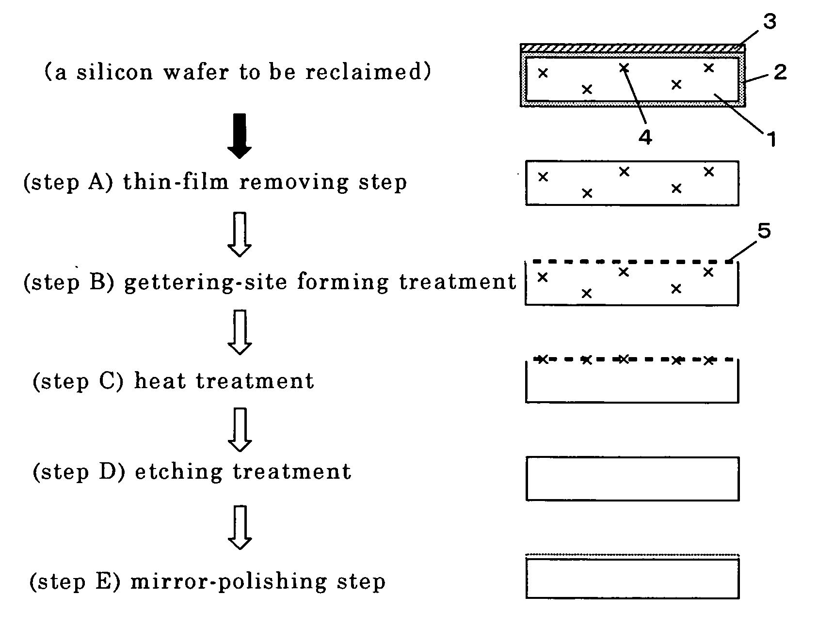
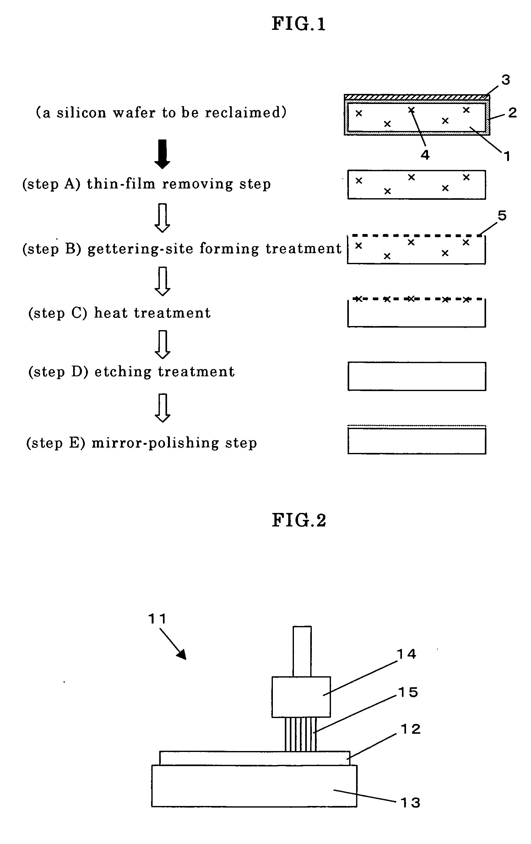
[0007] In order to accomplish the above object, according to the present invention, there is provided a method for reclaiming a silicon wafer in which a thin film has been formed on its surface, at least, comprising a thin-film removing step for removing the thin film having been formed on the silicon wafer and a mirror-polishing step for mirror-polishing at least one side of the thin-film-removed silicon wafer, wherein, before performing the mirror-polishing step, gettering-site forming treatment for applying damage load to at least one side of the silicon wafer is performed and then the silicon wafer is subjected to heat treatment, thereby impurities inside the silicon wafer are reduced.
[0008] By reclaiming a silicon wafer using such a method, a thin film such as a metal thin film having been formed on a silicon wafer can be removed, and impurities having diffused inside the wafer can be also reduced certainly through the use of gettering effect. Therefore, even such a contaminated silicon wafer as metal impurities having diffused inside the wafer after used in steps for producing semiconductor devices have become possible to be reclaimed easily, and extremely clean silicon wafers having very little metal contamination can be stably obtained.

Problems solved by technology

However, in the case of reclaiming a silicon wafer by using such a method, there has been a risk that metal ions dissolved at a high concentration in the chemical liquid adhere to the wafer again during immersing the wafer and thereby re-contamination is caused.
However, copper cannot be removed with such chemicals having been used conventionally as described above, and in the case that a wafer to which copper adheres is subjected to reclaiming treatment, there is possibility that the treatment process in itself is contaminated with copper and thereby other products are also contaminated with copper.
Therefore, it has been thought that it is difficult to reclaim a silicon wafer to which a copper film has adhered.
However, in the case of copper (impurities) having diffused inside the wafer, it is impossible to remove it perfectly.
Therefore, there is a problem that if the reclaimed polished wafer is subsequently used in steps for producing semiconductor devices and so forth, such troubles as lowering yield are caused.

Method used


Image

  • Silicon wafer reclamation method and reclaimed wafer
  • Silicon wafer reclamation method and reclaimed wafer
  • Silicon wafer reclamation method and reclaimed wafer

Examples


experiment 1

(Experiment 1)

[0048] First, four silicon wafers with a 300-mm diameter were prepared. And, after immersing these silicon wafers in a mixed solution of sulfuric acid and hydrogen peroxide having a 1000-ppm copper concentration, the wafers were heated at 700° C. for 1 hour. Thereby, silicon wafers that were purposely contaminated with copper inside the wafers were prepared.

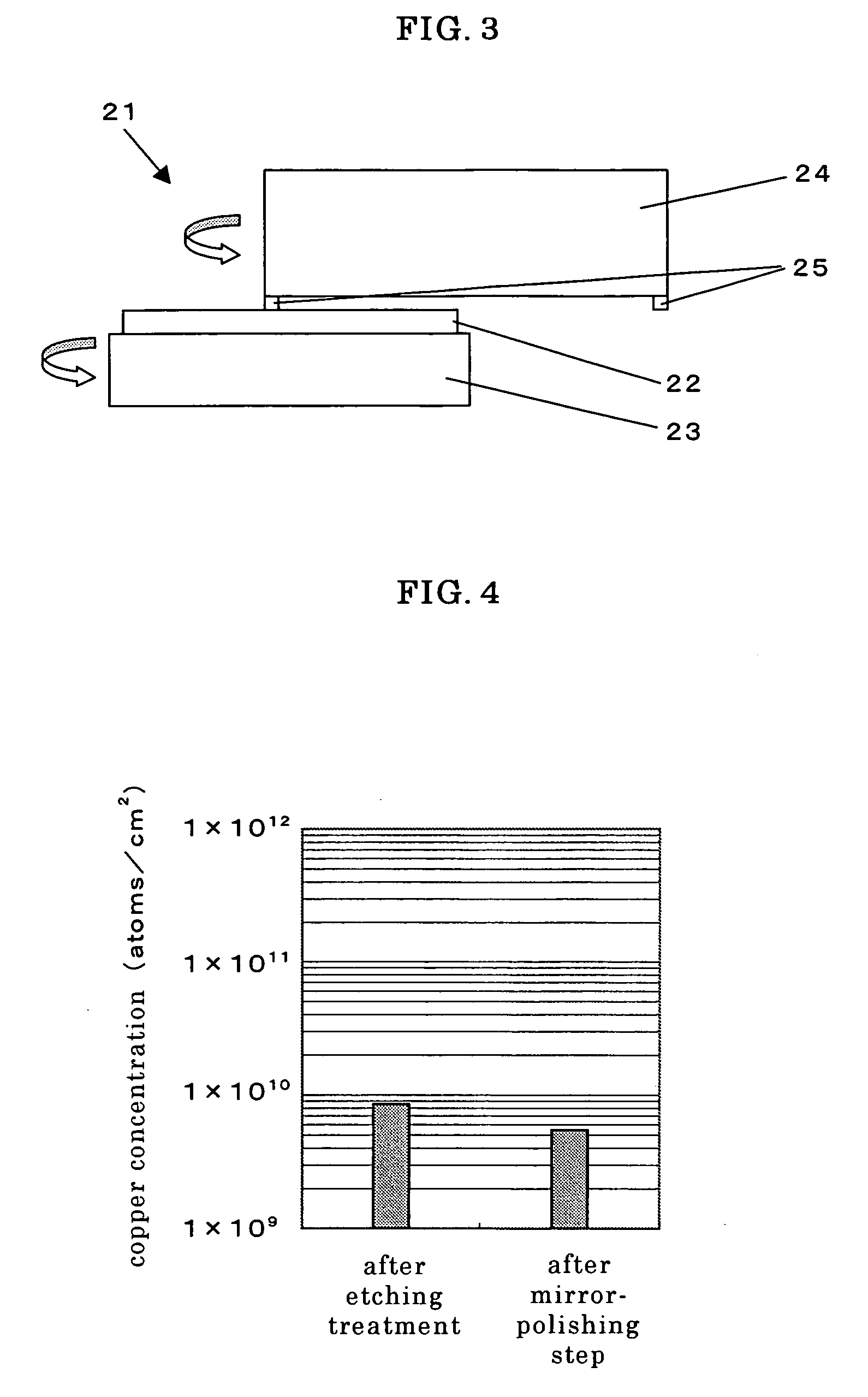
[0049] First, a wafer among the silicon wafers purposely contaminated with copper was subjected to sandblasting using the blast apparatus 11 as shown in FIG. 2 and thereby gettering sites were formed in the wafer surface. At this time, alumina grains with an average grain diameter of about 5 μm were used as a polishing agent. Next, the silicon wafer subjected to the gettering-site forming treatment was subjected to heat treatment by heating the wafer up to 650° C. and holding it for 1 hour and then cooling it down at a cooling rate of 4° C. / min. Then, the surface of the silicon wafer was etched and removed by 10 μm...

experiment 2

(Experiment 2)

[0050] Next, another silicon wafer purposely contaminated with copper as described above was subjected to surface-grinding using the surface-grinding apparatus 21 as shown in FIG. 3 and thereby gettering sites were formed in the wafer surface. At this time, as a grind stone, diamond grains in which those with grain diameters of about 2-6 μm having been fixed with resin were used. Then, after subjecting the silicon wafer to heat treatment and etching treatment as performed in the above-described Experiment 1, the copper concentration of the obtained silicon wafer was measured with the same method as above. As a result, it was found that the copper concentration of the wafer was 1.22×10¹⁰ atoms / cm2.

experiment 3

(Experiment 3)

[0051] For the comparison, another silicon wafer purposely contaminated with copper as described above was only etched by 10 μm with 48% NaOH, and the copper concentration of the obtained silicon wafer was measured by the same method to above. As a result, it was found that the copper concentration of the wafer was 2.01×10¹² atoms / cm2. Furthermore, the other silicon wafer purposely contaminated with copper as prepared above was subjected to heat treatment at 650° C. for 1 hour, etched by 10 μm with 48% NaOH, and the copper concentration of the obtained silicon wafer was measured by the same method as above. As a result, it was found that the copper concentration of the wafer was 1.25×10¹² atoms / cm2.

[0052] From the results of the Experiments 1-3, it can be confirmed that impurities inside a silicon wafer can be drastically reduced by subjecting the wafer to the gettering-site forming treatment and the heat treatment.

[0053] As described above, by a reclaiming method of...


PUM

PropertyMeasurementUnit
temperatureaaaaaaaaaa
diameteraaaaaaaaaa
grain diametersaaaaaaaaaa

Abstract

The present invention is a method for reclaiming a silicon wafer in which a thin film has been formed on its surface, at least, comprising a thin-film removing step for removing the thin film having been formed on the silicon wafer and a mirror-polishing step for mirror-polishing at least one side of the thin-film-removed silicon wafer, wherein, before performing the mirror-polishing step, gettering-site forming treatment for applying damage load to at least one side of the silicon wafer is performed and then the silicon wafer is subjected to heat treatment, thereby impurities inside the silicon wafer are reduced. Thereby, there is provided a method for reclaiming a silicon wafer, in which a thin film such as a metal thin film having been formed on a silicon wafer can be removed, and impurities having diffused inside the wafer can be also reduced, thereby silicon wafers having very little metal contamination can be stably obtained.

Description

TECHNICAL FIELD [0001] The present invention relates to a method for reclaiming a silicon wafer used in steps for producing semiconductor devices and so forth to be in a usable state again, and particularly relates to a method for reclaiming a silicon wafer in which metal such as copper is used as a metal thin film for wiring. BACKGROUND TECHNOLOGY [0002] In a silicon wafer used in steps for producing semiconductor devices and so forth, an insulator film such as SiO2 or a metal film for wiring such as Al, W, or Ti is generally deposited. For reclaiming such a silicon wafer as used in steps for producing devices and so forth, such a reclaiming method as immersing a silicon wafer in a chemical liquid such as a hydrofluoric acid or a sulfuric acid to dissolve and remove various types of thin films having deposited on the wafer, and then subjecting at least one side of front and back sides of the wafer to mirror-polishing has been conventionally used. However, in the case of reclaiming ...

Claims


Application Information

Patent Timeline
Patent Type & Authority Applications(United States)
IPC IPC(8): B44C1/22C03C25/68C23F1/00H01L21/322H01L21/02H01L21/304
CPCH01L21/02032H01L21/3221H01L21/02079H01L21/322
Inventor UCHIDA, TAKANOBUIIJIMA, KAZUHIDEYAMAZAKI, TETSUOTOMARU, SHINICHIMARUYAMA, FUMIAKI
Owner MIMASU SEMICON IND CO LTD
Learn More